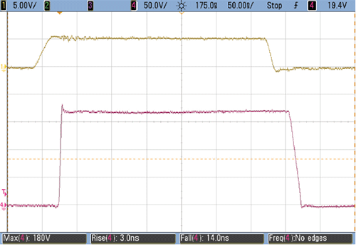
 EPC9003C的波形图 operation as a 170 V to 5 V / 5 A (100 kHz) buck converter
CH1: PWM Input – CH4: (VOUT) Switch node voltage
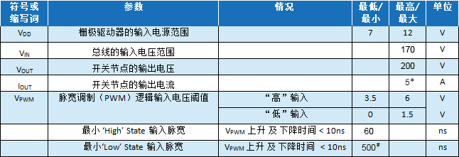 * Assumes inductive load, maximum current depends on die temperature – actual maximum current with be subject to switching frequency, bus voltage and thermal cooling.
# Dependent on time needed to ‘refresh’ high side bootstrap supply voltage.