EPC9040 : 100 V Development Board for
Enhancement Mode Monolithic Half-Bridge
Greater than 97% System Efficiency at 22 A
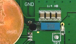
The EPC9040 development board has a 100 V maximum device voltage, 15 A maximum output current, in a half-bridge topology with onboard gate drives, featuring the EPC2104 eGaNIC (Enhancement-mode Gallium Nitride Integrated Circuit).
The purpose of this development board is to simplify the evaluation process of the EPC2104 eGaNIC by including all the critical components on a single board that can be easily connected into any existing converter.