EPC9048C: 200 V, 15 A Half-Bridge Development Board
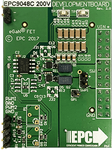
The EPC9048C development board is a 200 V maximum device voltage, 15 A maximum output current, half bridge with onboard gate drives, featuring the EPC2034C enhancement mode (eGaN®) field effect transistor (FET).
The EPC9048C development board is 1.5” x 2” and contains two EPC2034C eGaN FETs in a half bridge configuration. The gate driver used on this board is ON Semi’s NCP51820.
To simplify the evaluation process of the EPC2034C GaN FET, all the critical components and layout for optimal switching performance are implemented. Video: How to Turn an EPC Development Board into a Prototype
Status: Obsolete
The GaN Experts recommend EPC9099 for new designs