eGaN Technology Reliability and Physics of Failure - Examining eGaN Field Reliability
技术分享GaN技术杂谈 – Chris Jakubiec
7月 18, 2016
Examining eGaN® Field Reliability
Efficient Power Conversion (EPC) Corporation’s enhancement-mode gallium nitride (eGaN®) FETs and integrated circuits (ICs) are finding their way into many end user applications such as LIDAR, wireless charging, DC-DC conversion, RF base station transmission, satellite systems, and audio amplifiers.
Field reliability is the ultimate metric that corroborates the quality level of eGaN® FETs and ICs that have been deployed in customer applications. In our first installment we provided an overview of eGaN FET field reliability which included 6 years of volume production shipment, and greater than 17 billion total device hours recorded. A subsequent calculated Failure In Time (FIT – failures in 109 hours) of approximately 0.24 FITs shows excellent field reliability performance to date.
eGaN® FET electrical performance as well as reliability has been significantly enhanced by eliminating the package that traditional MOSFETs have been surrounded by. Removing the package around the die results in less variables that potentially contribute to field reliability issues such as mold compound, substrates, bond wires, and die attach materials. Additionally, eGaN FETs are resistant to moisture related issues of packaged devices, as they are well protected by passivation layers.
EPC performs a thorough root cause analysis of all returned field failures. As of the writing of our first installment (February 2016) 127 field failures have been investigated. Of the 127 field failures, 37 devices passed electrical testing with no anomalies detected, and were classified as good units. Figure 1 below shows the breakdown of analyzed failures grouped into root cause categories. The next three sections will go into more details describing the types of field failures that have been analyzed, as well as some recommendations to prevent such issues in the field.
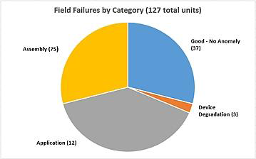
Figure 1: Field failure breakdown by root cause category
Assembly Failures
Device assembly and handling accounted for the highest number of field returns, with 75 units recorded in this category.
Improper control of the amount of solder paste and flux released during assembly, together with inadequate rinsing and curing of the flux made up 36 of the field failure units in this category. Flux that has not been properly rinsed and dried can accumulate in the areas between the solder balls, and has the potential to form dendrites which can create conductive leakage paths and lead to device failures. For high reliability assembly it is advised to rinse all residual flux underneath the die, and perform a high temperature dry curing step before applying any power to the device. Figure 2 shows dendrites connecting two terminals within uncured flux.
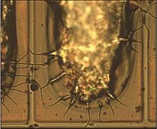
Figure 2: eGaN FET showing dendrite formation due to residual flux.
Die tilt issues can arise due to poor stencil design resulting in uneven solder paste volume release over the PCB pads. Vibration during assembly, reflow profile, and PCB solder mask design are other factors that can contribute to tilted die.
Figure 3 and Figure 4 below show an example of a poor assembly versus a properly mounted eGaN® device. EPC provides solder stencil, PCB land pattern, and solder standoff height recommendations for each device in the datasheets. Optimizing solder standoff height can help to provide additional space for rinsing of residual flux, and can also reduce thermo-mechanical stresses by adding compliance to the solder joints thus improving overall temperature cycling performance.

Figure 3: Tilted die trapping residual solder flux
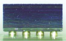
Figure 4: Properly mounted device
Die corner chipping was found to be the cause of failure for 27 units in the field. Chip-scale packages have many significant advantages over traditional semiconductor packages. There is no resistance, inductance, or size added to the transistor or IC. There are also fewer interfaces between different materials such as copper, mold compound, and solder that lead to higher field failure rates. Chip-scale packages as a consequence have the die exposed to the environment. In order to insure that each device is mechanically acceptable upon receipt by the customer, EPC has automated optical inspection tools in production to screen out any mechanical damage prior to tape and reel and shipment. Device assembly by the customer using automated tools such as pick and place must be programmed and aligned to avoid mechanical damage such as corner chipping or die cracks. In the 27 failures due to chipping, it was found that the PCB placement tool that was inserting components around the eGaN® device did not have adequate clearance to avoid hitting and damaging the die. Figure 5 below shows an example optical microscope image of a field failure due to die chipping.
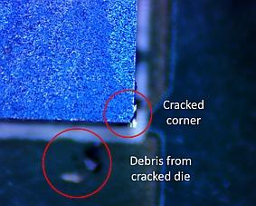
Figure 5: Field failure showing die corner chipping
Twelve failures were found to be related to inadequate amount of solder paste on the PCB pads during device assembly. The root cause was determined to be vias near solder pads that had not been tented during the PCB manufacturing. Tenting uses a layer of solder mask to cover the via opening and prevent a path for which solder could flow. An uncovered via adjacent to a pad can pull the solder paste down inside the via during high temperature reflow, leaving a lower volume of solder paste on the solder pad available to make contact with the device solder balls. Figure 6 shows a diagram of a tented via, and an example optical image of a PCB where the vias have been left uncovered.
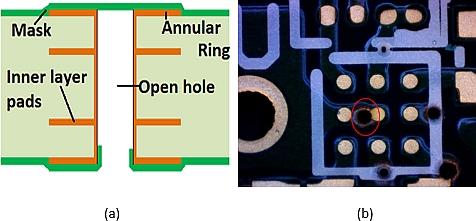
Figure 6: (a) Diagram of via with solder mask tent covering, (b) PCB showing uncovered via
Customers converting from traditional MOSFET packages to eGaN® chip-scale packages, are often required to learn techniques for assembling small packages and tighter solder geometries. Solder paste type, solder stencil, solder flux, board cleanliness, via design, solder mask, and solder joint standoff height are key parameters that must be understood to ensure assembly and board level reliability of eGaN devices. EPC has published assembly guides and videos on their website to help customers with proper assembly and rework: Assembly Resources
Application Failures
For a total of 12 field failures, the root cause was related to an application issue. Eleven of the field failures were damaged due to the electrical overstress resulting from voltage overshoot in a circuit layout that had too much parasitic inductance. Transient overvoltage can lead to device degradation observed as increased leakage currents or on state resistance, as opposed to DC overstress conditions which typically show up as completely inoperable devices.
The very low capacitance and extremely fast switching edge rates of eGaN® devices requires careful layout of PCBs to minimize common source inductance (CSI), the inductance in the gate-to-source loop, and power loop inductance (See Figure 7). Figure 8 demonstrates the impact on switching waveform overshoot in a high frequency application, by reducing loop inductance of the PCB layout from 1.6nH to 0.4nH. The peak transient voltage due to the high frequency power loop inductance is reduced from 100% to 30% of the steady state value respectively.
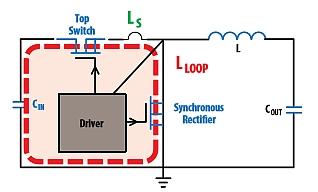
Figure 7: Synchronous rectifier showing parasitic inductances (L
S is common source inductance) (L
Loop is high frequency power loop inductance)
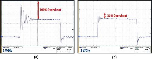
Figure 8: (a)High frequency switching waveform of eGaN
® FET design with power loop inductance L
Loop = 1.6 nH, (b) High frequency switching waveform of eGaN FET design with power loop inductance L
Loop = 0.4nH EPC eGaN FET EPC2015 Synchronous Rectifier Circuit (V
IN = 12 V, V
OUT = 1.2 V, F = 1 MHz)
Similarly, increased common source inductance and non-optimal resistance at the gate drive circuit can result in voltage overshoots and ringing that can cause device failures. Optimization of the gate drive resistance and reduction of the gate loop inductance results in significantly less voltage overshoot as seen in Figure 9 below.
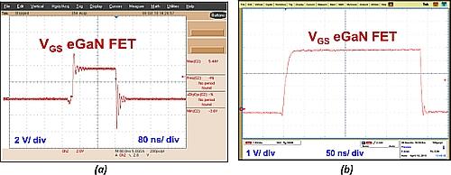
Figure 9: (a)Non-optimized gate drive circuit (b)Optimized gate drive circuit, EPC eGaN FET EPC2010 Synchronous Rectifier Circuit
For guidelines on optimizing PCB layout using eGaN® FETs refer to the following EPC publication: Optimizing PCB Layout
Intrinsic Device Failures
Intrinsic device failures account for a lower percentage of field returns with only 3 units documented, however it is equally important that root cause is determined. Based on these 3 field failure units together with over 17 billion device hours, the calculated FIT rate is approximately 0.24 FITS (60% confidence interval).
Dynamic RDS(ON) is a mechanism that can adversely affect older generation GaN devices, as a result of carrier trapping in the basic material layers. The on state resistance of a GaN FET can shift when subjected to high drain voltage over long periods of time due to the activation of these traps. This phenomenon must be understood both by the FET manufacturer and the end user to design in sufficient guard band to accommodate. EPC has ongoing efforts to improve the material properties that reduce carrier trap concentrations, and thus limit the dynamic RDS(ON) to a negligible effect. See published Phase 6 & 7 reliability reports on the EPC website for further analysis: eGaN FET Reliability
The very low field failure rate of eGaN® devices demonstrates when properly assembled and operated, GaN technology is inherently reliable in many end user applications. In out next installment we will take a look into what types of stress tests are performed to qualify an eGaN device. The collection of data includes thousands of devices tested over millions of stress hours for GaN technology, environmental conditions, and thermo-mechanical stresses. Early life failure rate data will also be presented. We will show that GaN technology passes similar levels of rigorous stress testing as any traditional MOSFET.
eGaN is a registered trademark of Efficient Power Conversion Corporation