客户可以在我们的网页 注册 ,定期收取最新消息包括全新产品发布、应用文章及更多其它资讯。如果你错过了已发布的资料,你可浏览以下的文档。
低压 GaN FET 可实现更小、冷却要求最小化和效率更高的解决方案
与采用传统的硅基功率 MOSFET的应用相比,低压 GaN FET(即 100 V)可实现更小,冷却要求最小化和效率更高的解决方案。 本文讨论了氮化镓器件如何应对动态性能需要重复且可靠的表征的挑战。 定制氮化镓夹具和测试板的机械和电气设计仔细、周全,就可以克服其中许多挑战,使您能够在设计功率转换器时,自信地使用这些新型宽能隙器件。
Power Electronics News
2023年7月
阅读文章
阅读全文
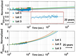
Transient voltage overshoot is a common phenomenon in GaN high electron mobility transistors (HEMTs) under high slew rate switching conditions. The dynamic parametric instability under such stress is a critical concern for GaN applications. This work, for the first time, accurately characterized the evolution of dynamic on-resistance (RDS(on)) in GaN HEMTs under repetitive voltage overshoot up to billions of switching cycles. The dynamic RDS(on) increase was found to be the dominant device degradation under overvoltage switching. Such findings were obtained from a high-frequency, repetitive, unclamped inductive switching (UIS) test with active temperature control and accurate in-situ RDS(on) monitoring. A physics-based model was proposed to correlate the dynamic RDS(on) drift with the peak overvoltage, and a good agreement with experimental data was achieved. This model was further used to project the lifetime of GaN HEMTs. For 100 V rated GaN HEMTs switched under 100 kHz and 120 V spikes, the model projects less than 10% dynamic RDS(on) shift over 25 years of continuous operation. This work addresses the major concerns of overvoltage switching reliability of GaN HEMTs and provides new insights of the electron trapping mechanism.
IEEE Xplore
Ruizhe Zhang, Ricardo Garcia, Robert Strittmatter, Yuhao zhang, Shengke Zhange
Read article (IEEE subscription required)
阅读全文
Based on the authors' years of extensive experience, this is an authoritative overview of Wide Bandgap (WBG) device characterization.
EL SEGUNDO, Calif. – September 2018 – Efficient Power Conversion Corporation (www.epc-co.com) announces the publication by the Institution of Engineering and Technology of Characterization of Wide Bandgap Power Semiconductor Devices co-authored by EPC Senior Applications Engineer, Dr. Edward A. Jones. This textbook provides essential tools to assist researchers, advanced students, and practicing engineers in performing both static and dynamic characterization of WBG devices, particularly those based on using silicon carbide (SiC) and gallium nitride (GaN) power semiconductors. The book presents practical considerations for real applications and includes examples of applying the described methodology.
阅读全文