客户可以在我们的网页 注册 ,定期收取最新消息包括全新产品发布、应用文章及更多其它资讯。如果你错过了已发布的资料,你可浏览以下的文档。
与采用传统硅器件的转换器相比,采用氮化镓基高电子迁移率晶体管 (HEMT) 具有许多材料和性能优势,已广泛用于消费和工业用功率转换领域。氮化镓器件在更高的开关频率下提高了功率转换效率,进而实现更低的系统成本和更高的功率密度。随着功率密度的增加,散热分析和热建模变得至关重要。我们将在本文分享EPC的热量计算器。 EPC公司制造增强型 GaN HEMT 和集成电路,例如支持多种转换器的半桥器件。
Power Electronics News
2023年11月
阅读文章
阅读全文
低压 GaN FET 可实现更小、冷却要求最小化和效率更高的解决方案
与采用传统的硅基功率 MOSFET的应用相比,低压 GaN FET(即 100 V)可实现更小,冷却要求最小化和效率更高的解决方案。 本文讨论了氮化镓器件如何应对动态性能需要重复且可靠的表征的挑战。 定制氮化镓夹具和测试板的机械和电气设计仔细、周全,就可以克服其中许多挑战,使您能够在设计功率转换器时,自信地使用这些新型宽能隙器件。
Power Electronics News
2023年7月
阅读文章
阅读全文
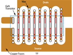
In this article, different power loop layouts are analyzed with simultaneous considerations for thermal management and electric parasitics.
The results show that an improved layout can provide a significant reduction in operating temperature rise while maintaining electrical performance benefits.
EE Power
October, 2022
Read Article
阅读全文
宜普电源转换公司(EPC)新推线上论坛,为工程师提供产品信息、答疑解难和分享採用氮化镓技术的应用现状和发展趋势。
宜普电源转换公司宣布新推"GaN Talk支持论坛",为工程师提供产品信息和技术支持,从而了解氮化镓(GaN)技术的应用现状和发展趋势。该论坛专为工程师、工程专业学生和所有氮化镓技术爱好者而设,为用户答疑解难和提供互相交流的平台。提问可以用主题类别、热门话题或最新帖子搜索。除了提问外,用户还可以在论坛使用帖子中的"分享"链接参看所有之前的提问和反馈。
阅读全文
宜普电源转换公司(EPC)为工程师提供更多的设计工具、模型和性能仿真器,用于基于高性能氮化镓器件的设计。
EPC公司宣布推出GaN Power Bench™设计工具,帮助工程师实现基于氮化镓器件的设计的最高性能。eGaN® FET和IC具有快速开关、高效和小尺寸等优势,可满足当今前沿应用对功率密度的严格要求。GaN Power Bench工具可帮助设计工程师为各种应用选择最合适的氮化镓器件、模拟和优化设计的散热性能,并提供应用实例和相关文档,从而可以快速、轻松地实现最佳设计的理想性能。
阅读全文
This article discusses the challenges that thermal management raises due to increase power density, especially with chip-scale packaging (CSP). What is sometimes overlooked, however, is that CSP eGaN® power FETs and integrated circuits have excellent thermal performance when mounted on standard printed circuit board (PCBs) with simple methods for attaching heat sinks. Simulations, supported by experimental verification, examine the effect of various parameters and heat flow paths to provide guidance on designing for performance versus cost.
Bodo’s Power Systems
February, 2021
Read article
阅读全文
Gallium nitride (GaN) transistors have been in mass production for over 10 years. In their first few years of availability, the fast switching speed of the new devices – up to 10 times faster than the venerable Si MOSFET – was the main reason for designers to use GaN FETs. As the pricing of GaN devices normalized with the MOSFET, coupled with the expansion of a broad range of devices with different voltage ratings and power handling capabilities, much wider acceptance was realized in mainstream applications such as DC-DC converters for computers, motor drives for robots, and e-mobility bikes and scooters. The experience gained from the early adopters has led the way for later entrants into the GaN world get into production faster. This article is the first in a series of articles discussing three topics that can help power systems designers achieve the most out of their GaN-based designs at the lowest cost. The three topics are: (1) layout considerations; (2) thermal design for maximum power handling; and, (3) EMI reduction techniques for lowest cost.
Bodo’s Power Systems
January, 2021
Read article
阅读全文