Rethinking Server Power Architecture in a Post-Silicon World: Getting from 48 Vin – 1 Vout Directly
GaNの話 – David Reusch, Ph.D.
7 26, 2016
Alex Lidow, Ph.D., CEO and Co-founder
David Reusch, Ph.D., Executive Director of Applications Engineering
John Glaser, Ph.D., Director of Applications Engineering
The demand by our society for information is growing at an unprecedented rate. With emerging technologies, such as cloud computing and the internet of things (IoT), this trend for more and faster access to information is showing no signs of slowing. What makes the transfer of information at high rates of speed possible are racks and racks of servers, mostly located in centralized data centers.
In 2014, data centers (in the U.S.) consumed about 100 billion kilowatts hours (kWh) of energy and it is projected by the Natural Resources Defense Council (NRDC) that data center electricity consumption will increase to roughly 140 billion kilowatt-hours annually by 2020, the equivalent annual output of 50 power plants.
The power needed to support this rapidly growing demand comes from our electrical grid, and goes through multiple conversion stages before it actually feeds the remaining energy into a digital semiconductor chip. In figure 1 is an illustration of this “journey.” Also shown in this figure are the losses due to the transmission and conversion of electricity – from the power plant to the computer chip that does all the work.
Multiplying these efficiency numbers shows that the power grid needs to supply 150 watts of power to meet the demands of a digital chip that may need only 100 watts of power. Therefore the combined waste across the U.S. due to power conversion for servers is 33 billion kWh, equivalent to almost a dozen power plants. But the overall wasted energy within the server farm is even more, because every watt of power loss through power conversion is actually energy that is converted into heat, and removing this heat demands even more power.
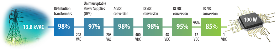
Figure 1: Typical multi-stage power conversion architecture used in modern server farms, which takes 150 watts of power from the electrical grid to supply 100 watts to a digital processor used in servers.
Whereas the electrical grid has been around for more than a century, the various stages of conversion have been built with technologies based on the semiconductors developed post World War II. These semiconductors are based on silicon crystals, and it is the properties and limitations of silicon that shaped the architecture of figure 1.
In this article, we will demonstrate the benefits of enhancement-mode gallium nitride (eGaN® technology) based power converters in solutions for existing data center and telecommunications architectures centering around an input voltage of 48 VDC with load voltages as low as 1 VDC. We will explore the capability of high performance GaN power transistors to enable new approaches to power data center and telecommunications systems with higher efficiency and higher power density than possible with previous Si MOSFET based architectures.
Getting from 48 VIN – 1 VOUT Directly
Since the adoption of the 12 V intermediate bus architecture (IBA), bus converters are currently approaching about an order of magnitude increase in output power, from around 100 W to current designs of around 1 kW in a quarter brick footprint. This means that the amount of current on the 12 V bus to the POL converters has also increased by a factor of 10 and, without reductions in busing resistance, a two order of magnitude increase in busing conduction losses follows. GaN technology-based solutions have already demonstrated significant efficiency improvements compared to silicon based solutions in traditional IBA systems.
However, with the increasing conversion losses in the 48 VIN bus converter, the mounting 12 V busing losses on the motherboards, and the higher performance of GaN technology, different architectures may now be considered, such as going directly from 48 VIN to load using non-isolated POL converters, as shown on the bottom of figure 2.

Figure 2: Intermediate bus architecture (IBA) and a direct conversion DC bus architecture.
The first approach evaluated to convert 48 VIN directly to 1 VOUT is a traditional buck converter. The buck converter is one the simplest topologies and the approach taken in the vast majority of current 12 VIN systems. For the 48 V input, an 80 V eGaN monolithic half-bridge IC (EPC2105), embedded in an EPC9041 demonstration board, was selected for the much higher step-down ratio. A second approach to convert 48 VIN direct to 1 VOUT, from Texas Instruments, uses a transformer-based design to improve converter efficiency. An LMG5200 GaN-based half bridge is used on the 48 VIN input side, and four 30 V EPC2023 eGaN FETs are used on the low voltage output side.
The efficiencies and power densities of the two 48 VIN to 1 VOUT designs are shown in figure 3. The buck converter efficiency is that of the entire power train, including the inductor (Würth Elektronik 744 301 033), capacitors, and PCB losses. At a switching frequency of 300 kHz, a peak efficiency of 84% is achieved, and at 20 A the efficiency is around 83.5%. The power density of the buck building block (excluding controller) is approximately 300 W/in3. For the transformer-based approach operating at 600 kHz, efficiencies over 90 % are achieved, with the efficiency almost 88% at 50 A of output current. For the transformer-based building block (excluding controller), the power density is approximately 80 W/in3.
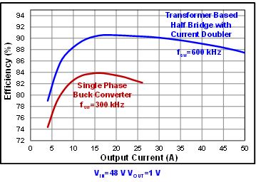
Figure 3: Efficiency and power density of eGaN based POL converters,
V
IN=48 V to V
OUT=1 V.
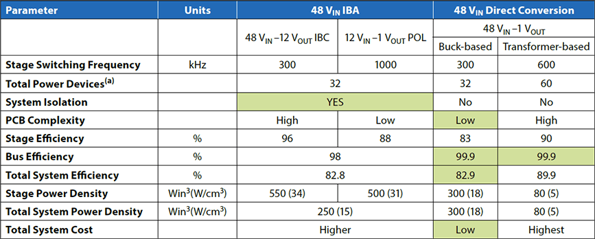
A comparison of estimated efficiencies and power densities for the single stage 48 VIN to 1 VOUT POL converters and the traditional two-stage IBA approach using the best GaN technology-based design is shown in figure 4, and summarized in table 1 (Silicon-based solutions are significantly less efficient than these GaN technology-based solutions). The GaN IC-based IBA’s power converters have an estimated 1.5% efficiency improvement over the direct 48 VIN to 1 VOUT conversion for the buck-based approach. However, when adding in the losses from the 12 V bus, estimated to be 2%, the total system efficiencies are very similar. The traditional IBA approach and 48 VIN direct conversion buck-based approach have similar power densities. For the 48 VIN transformer-based approach, the system efficiency is over 7 % higher than the traditional IBA approach and the system has a lower power density, about a third of the conventional IBA GaN based approach.
The DC bus architecture also has a potential cost advantage, since the cost of the IBC can be eliminated and the cost increase of the 48 VIN POL converter over the 12 VIN POL converter will be minimal as they use a similar number of power devices, controllers, and drivers.
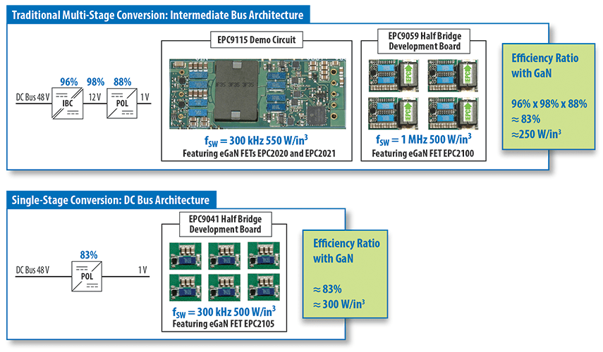
Figure 4: Performance comparisons of GaN technology-based 48 V
IN intermediate bus architecture and 48 V
IN DC bus architecture
(a) Scaled to 500 W of output power.
Table 1: Summary of 48 V
IN intermediate bus architecture and 48 V
IN DC bus architecture performance comparisons
In figure 5 we revisit figure 1 while applying the single-stage efficiencies demonstrated with eGaN FET and IC based designs. The direct savings by eliminating just the last stage in the server farm power architecture is not only a cost reduction, but also a reduction of power consumed between 7-15% depending on the GaN-based approach. This correlates to direct savings of up to 21 billion kWh per year when compared with silicon-based solutions. This savings is increased further when air conditioning energy costs inside the server farm are added, bringing the total to almost 25% of the 140 billion kWh consumed by servers in the U.S. alone.
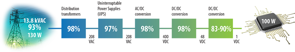
Figure 5: eGaN devices enable the elimination of an entire stage in the power conversion journey, reducing total server farm losses by up to 10%.
Conclusion
The impact of eGaN technology in our post-silicon world is even greater than the savings possible in U.S. server farms today and is but one example of the impact that this new, emerging technology makes to the efficient use of electrical power. eGaN technology provides a path to higher performance semiconductors, re-opening the possibilities of Moore’s Law for driving innovation – just as Moore’s Law falls off the tracks. For example, eGaN technology is enabling new applications such as wireless power transmission, 5G cellular, autonomous vehicles, and colonoscopy pills. And, as the electronics industry gains experience and knowledge in the inherent attributes high performance capabilities, the resulting high performance eGaN semiconductor devices will enable many unforeseen applications, just as silicon, its predecessor, brought about in the post-WWII era.
eGaN® FET is a registered trademark of Efficient Power Conversion Corporation.
General Reference
[1] D. Reusch and J. Glaser, DC-DC Converter Handbook, Power Conversion Publications, 2015. ISBN 978-0-9966492-0-9