EPC9084: 300 V, 4 A Half-Bridge Development Board
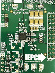
The EPC9084 development board is a 300 V maximum device voltage, 4 A maximum output current, half bridge development board. The EPC9084 board measures 2” x 2” and contains a 300 V EPC2050 enhancement mode (eGaN®) field effect transistor (FET) with the Silicon Labs SI8274GB1 gate driver.
To simplify the evaluation process of the EPC2050 GaN FET, all the critical components are included on a single board that can be easily connected into any existing converter.
This board may be used for applications where high efficiency can enable a significant performance advantage as well as a size and weight reduction such as multi-level AC/DC power supplies, electric vehicle on-board charging, and solar power inverters.
Status: Obsolete
The GaN Experts recommend EPC90121 for new designs