EPC9099: 200 V, 15 A Half-Bridge Development Board
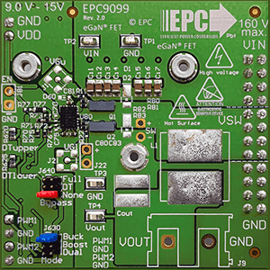
The EPC9099 development board is a 200 V maximum device voltage, 15 A maximum output current, half bridge with onboard gate drives, featuring the EPC2215 enhancement mode (eGaN®) field effect transistor (FET).
The EPC9099 development board is 2” x 2” and contains two EPC2215 eGaN FETs in a half bridge configuration using the Texas Instruments LMG1210 gate driver.
To simplify the evaluation process of the EPC2215 GaN FET, all the critical components are included on a single board that can be easily connected into any existing converter. Video: How to Turn an EPC Development Board into a Prototype