EPC90120 - Development Board

EPC90120: 80 V, 10 A Development Board

EPC90120 Development Board

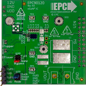
The EPC90120 development board is a 80 V maximum device voltage, 10 A maximum output current, half bridge with onboard gate drives, featuring the EPC2152 Integrated ePower Stage.

The EPC90120 development board is 2” x 2” and contains one EPC2152 Integrated ePower Stage in a half bridge configuration.

To simplify the evaluation process of the EPC2152, all the critical components and layout for optimal switching performance are implemented. Video: How to Turn an EPC Development Board into a Prototype

Ask and EPC Engineer a Question FAQ

Have a design question?
Ask a GaN Expert

EPC90120 Parameters Table
(1) Maximum input voltage depends on inductive loading, maximum switch node ringing must be kept under 80 V for EPC2152.
(2) Maximum current depends on die temperature – actual maximum current with be subject to switching frequency, bus voltage and thermal cooling.
(3) Limited by time needed to ‘refresh’ high side bootstrap supply voltage.
(4) When using the on board logic buffers, refer to the EPC2152 datasheet when bypassing the logic buffers.