EPC9055 - Development Board

EPC9055 : 100 V Half-Bridge Development Board

EPC Development Board

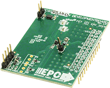
The EPC9055 development board is a 100 V maximum device voltage, 3 A maximum output current, in a half-bridge topology with onboard gate drives, featuring the EPC2106 enhancement mode (eGaN®) field effect transistor (FET).

The purpose of this development board is to simplify the evaluation process of the EPC2106 eGaN FET by including all the critical components on a single board that can be easily connected into any existing converter.

Ask and EPC Engineer a Question FAQ

Have a design question?
Ask a GaN Expert

EPC9055 Waveform Chart
Waveforms for operation as a 80 V to 5 V/ 3 A (500kHz) buck converter
CH1: VPWM Input voltage – CH2: (IOUT) Switch node current – CH4: (VOUT) Switch node voltage
EPC Development Board
* Assumes inductive load, maximum current depends on die temperature – actual maximum current will be subject to switching frequency, bus voltage and thermal cooling.
# Dependent on time needed to ‘refresh’ high side bootstrap supply voltage.