How to Design a Bi-Directional 1/16th Brick 48 V-12 V Converter Using Monolithic GaN ePower™ Stage
技術分享雜談GaN技術 – Alex Lidow, Ph.D.
十二月 14, 2020
Introduction
Brick DC-DC converters are widely used in data center, telecommunication and automotive applications, converting a nominal 48 V bus to (or from) a nominal 12 V bus. Advances in GaN integrated circuit (IC) technology have enabled the integration of the half bridge and gate drivers, resulting in a single chip solution that simplifies layout, minimizes area, and reduces cost.
This application note discusses the design of a digitally controlled bi-directional 1/16th brick converter using the integrated GaN power stage for 48 V-to-12 V application, with up to 300 W output power, and peak efficiency of 95%.
The standard dimension of the 1/16th brick converter is 33 x 22.9 mm (1.3 x 0.9 inch). The height limit for this design is set to 10 mm (0.4 inch).
Monolithic GaN ePower™ stage
The monolithic integration of GaN FETs and gate drivers offers improved performance and simplified board layout. It also reduces parasitic inductance and capacitances, and related losses.
Figure 1 (a) shows a simplified block diagram of the EPC2152 GaN ePower™ Stage [1]. The main power FETs are controlled by the integrated gate drivers. The IC also includes input buffers that accept logic levels from 3.3 V to 5 V. Other standard features are also included, such as power-on-reset (POR) and under-voltage-lockout (UVLO) functions, a high voltage signal level-shifter and a synchronous bootstrap FET [2]. A photo of the monolithic GaN power stage is shown in Figure 1 (b). Both power GaN FETs are 80 V rated, with 10 mΩ on-resistance.
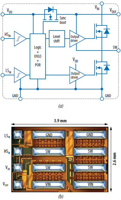 Figure 1. (a) Block diagram, and (b) photo of the monolithic GaN ePower stage, EPC2152 [1]
Design of the Bi-directional DC-DC converter
One of the key challenges in designing a high power 1/16th brick is the limited space. The integrated EPC2152 requires an area of just 18 mm2, leaving room for adequate decoupling capacitors that help achieve high efficiency.
A simplified schematic of the EPC9151 bi-directional capable 1/16th brick DC-DC converter is shown in Figure 2. It includes a two-phase synchronous buck power stage, a digital controller, current sensors and housekeeping power supply. A two-phase approach is selected so that the peak current requirement is reduced, and smaller magnetics can be used.
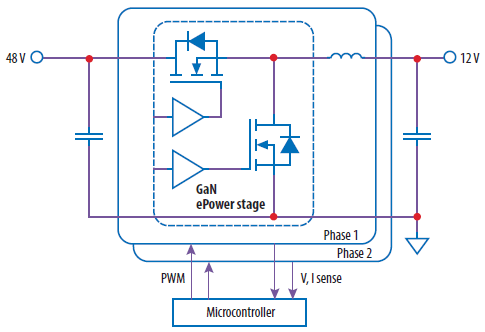 Figure 2. Schematic of the 1/16th brick bi-directional DC-DC converter
With the integrated power stage, it is easy to minimize the power loop inductance. The high frequency decoupling capacitors are placed next to the IC, using the optimum layout [4] technique, and the second layer of the printed circuit board (PCB) is a ground plane, as shown in Figure 3. Another two layers of ground plane are also included in this six-layer PCB, for better heat sinking as well as shielding for the voltage and current feedback signals.
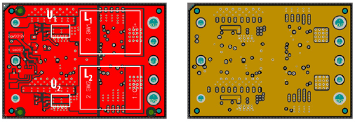 Figure 3. First two layers of the printed circuit board showing simplified layout using EPC2152
TDK B82559 series inductors [5] are used, with a dimension of 13 x 10.7 mm (0.51 x 0.42 inch), and a height of 5 mm or 6 mm. The 2.4 μH inductor has a saturation current rating of 16.5 A. Therefore, 500 kHz switching frequency is selected, resulting in 16.25 A peak current when converting 48 V to/from 12 V that satisfies the saturation current requirement.
Digital Control
A dsPIC33CK32MP102 digital controller from Microchip [6] is used. It is a 16-bit processor with a maximum CPU speed of 100 MIPS. The pulsewidth modulation (PWM) module can be configured in high-resolution mode, resulting in 250 ps resolution in duty cycle and dead times, allowing accurate adjustment of dead times to fully exploit the high performance of GaN FETs.
Digital average current mode control is implemented for both buck and boost modes. The current sensing circuitry consists of sense resistors and differential amplifiers. In this design, low loss 1 mΩ sense resistors and low-noise amplifiers MCP6C02 are used. The control block diagram is shown in Figure 4. The same current reference IREF is used for the two independent current loops. As a result, the current in both inductors will be regulated to the same value. The bandwidth of the two inner current loops are set to 10 kHz, and the outer voltage loop bandwidth is set to 2 kHz.
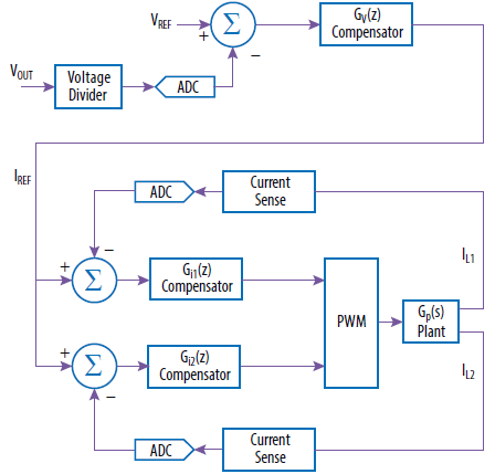 Figure 4. Control block diagram of the multi-loop 2-phase converter
Experimental Results
Figure 5 shows a photo of the EPC9151 1/16th brick converter mounted on the EPC9531 test fixture, as well as its bottom side. The total standoff height of the design is 9.1 mm, including 6 mm from the inductors, 1.6 mm from the PCB thickness, and 1.5 mm for the bottom component (0805 size capacitors).
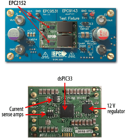 Figure 5. Top and bottom sides of the EPC9151 1/16thbrick converter
The EPC9531 shown in figure 5 (top), test fixture has additional input capacitance of 47 μF and output capacitance of 200 μF. These extra capacitances help maintain controller stability. The fixture also provides programming ports and USB communication.
With no heatsink and 1700 LFM airflow, the measured thermal steady state efficiency and loss are shown in Figure 6 (a) for buck mode, and Figure 6 (b) for boost mode. The peak efficiency is 95.5% for buck mode and 95.1% for boost mode. The maximum device temperature reached 89°C at maximum output power, as illustrated in the thermal image in Figure 7. In an environment with moderate airflow such as 400 to 800 LFM, a heatsink is necessary.
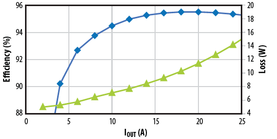
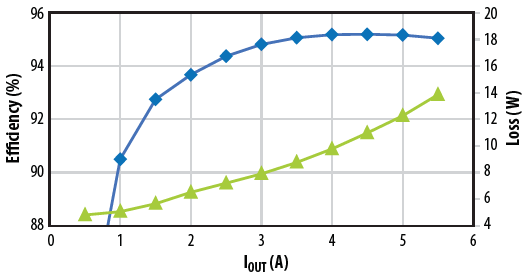 Figure 6. Measured efficiency and loss for the 1/16th brick converter: (a) VIN = 48 V, VOUT = 12 V (buck); and (b) VIN= 12 V, VOUT = 48 V (boost)
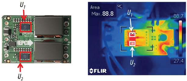 Figure 7. Thermal image of the 1/16th brick converter operating in thermal steady state. VIN = 48 V, VOUT = 12 V, 25 A output current, airflow 1700 LFM
Conclusions
This application note introduces a bi-directional high power EPC9151 1/16th brick converter using two EPC2152 monolithically integrated GaN power stages. It exemplifies a simpler layout and higher power density compared to state-of-art MOSFET designs. A 300 W 48 V to/from 12 V converter design is presented with 95% peak efficiency.
References
[1] “EPC2152 – 80 V, 10 A Integrated ePower™ Stage,” Efficient Power Conversion Preliminary Datasheet, Jan. 2020.
[2] M.A. de Rooij, J.T. Strydom, D.C. Reusch, “High Voltage Zero QRR bootstrap Supply,” United States Patent US9,667,245 B2, May 30, 2017.
[3] Y. Zhang and M. de Rooij, “300 W 48V-12V Digitally Controlled 1/16th Brick DC-DC Converter Using GaN FETs,” PCIM - Europe, July 2020.
[4] A. Lidow, M. De Rooij, J. Strydom, D. Reusch, and J. Glaser, GaN transistors for efficient power conversion, 3rd ed. John Wiley & Sons, 2019. ISBN: 978-1119594147.
[5] TDK. (2012). SMT power inductors, [Online]. Available: https://www.tdk-electronics.tdk.com/inf/30/db/ind_2008/b82559_a013.pdf.
[6] Microchip Technology Inc. (2019). 16-bit PIC Microcontrollers Family, [Online]. Available: https://www.microchip.com/designcenters/16-bit.