EPC9040:开发板

EPC9040: 采用增强型单片式半桥氮化镓器
件的100 V 开发板

Greater than 97% System Efficiency at 22 A

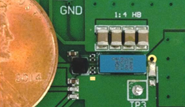
EPC9040 开发板的最高器件电压为100 V、最大输出电流为15 A,采用半桥拓扑并含板载栅极驱动器及特色产品增强型氮化镓集成电路 - EPC2104 eGaNIC

该开发板旨在于一块单板上包含所有重要元件以易于连接至任何现有的转换器,从而简化对EPC2104 eGaNIC进行评估的过程。

立即购买
购买 eGaN FET及集成电路


向GaN技术专家请教

有没有电路设计及相关的提问吗?
向GaN技术专家请教

EPC9040 Efficiency Chart典型效率: 48 VIN – 12 VOUT

EPC9040 Parameters Table* Maximum input voltage depends on inductive loading.
** Maximum current depends on die temperature – actual maximum current with be subject to switching frequency, bus voltage and thermal cooling.
Symmetrical eGaNIC intended for 50% duty cycle or low step-down ratio applications.
#受限于需要“更新”高侧自举电源电压的时间