EPC9040:開發板

EPC9040: 採用增强型單片式半橋氮化鎵器
件的100 V 開發板

Greater than 97% System Efficiency at 22 A

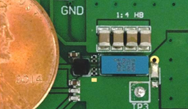
EPC9040 開發板的最高器件電壓爲100 V、最大輸出電流爲15 A,採用半橋拓撲幷含板載栅極驅動器及特色産品增强型氮化鎵集成電路 - EPC2104 eGaNIC

該開發板旨在於一塊單板上包含所有重要元件以易於連接至任何現有的轉換器,從而簡化對 EPC2104 eGaNIC進行評估的過程。

立即購買
購買 eGaN FET及積體電路

向GaN技術專家請教

有沒有電路設計及相關的提問嗎?
向GaN技術專家請教

EPC9040 Efficiency Chart 典型效率: 48 VIN – 1.2 VOUT

EPC9040 Parameters Table* Maximum input voltage depends on inductive loading.
** Maximum current depends on die temperature – actual maximum current with be subject to switching frequency, bus voltage and thermal cooling.
Symmetrical eGaNIC intended for 50% duty cycle or low step-down ratio applications.
#受限于需要“更新”高側自舉電源電壓的時間