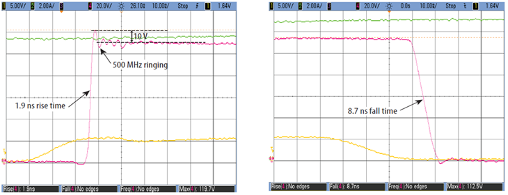
 110 Vから5 V/12 A(100kHz)へのバック・コンバータとして動作したときの波形
CH1:VPWM入力電圧、CH2:(IOUT)スイッチ・ノード電流、CH4:(VOUT)スイッチ・ノード電圧
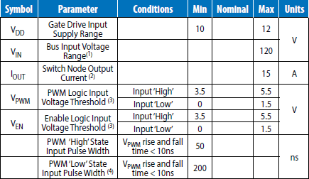 (1) Maximum input voltage depends on inductive loading, maximum switch node ringing must be kept under 150 V for EPC2033.
(2) Maximum current depends on die temperature – actual maximum current is affected by switching frequency, bus voltage and thermal cooling.
(3) When using the on board logic buffers, refer to the NCP51820 datasheet when bypassing the logic buffers.
(4) Limited by time needed to ‘refresh’ high side bootstrap supply voltage.