From Data Centers to Robotics: The Expanding Domain of GaN Power Electronics
技術分享雜談GaN技術 – Maurizio Di Paolo Emilio
五月 12, 2026
By Maurizio Di Paolo Emilio
The full article was originally published in EPDT
The history of power electronics has been a predictable cadence of material limits, architectural shifts, and a new semiconductor platform resetting expectations. Today that transition is happening again, this time with gallium nitride (GaN).
In a recent semiconductor podcast interview on TechSimplified TV, Alex Lidow, CEO and co founder of Efficient Power Conversion (EPC) and co inventor of the HEXFET power MOSFET, provided a rare long term view of how GaN is transforming the future of efficient power conversion. His message was clear and simple:
“Silicon’s running out of steam and when that happens, you’ve got to have something new come in. That's gallium nitride.”
This statement is not only a technical reality but also a strategic shift that we now see across AI infrastructure, robotics, satellites, consumer fast charging, and emerging electrified platforms.
Why Gallium Nitride Changes the Rules
The advantages of GaN begin at the atomic level. Compared with silicon, the stronger chemical bond between gallium and nitrogen produces a wider bandgap material capable of sustaining higher electric fields and supporting faster switching operation.
As Lidow explains: “Because the chemical bond is stronger, gallium nitride can withstand higher electric fields. That means power components can be made smaller, faster, and more efficient.”
Unlike silicon devices, GaN high‑electron‑mobility transistors (HEMTs) exploit a two‑dimensional electron gas (2DEG) formed at the AlGaN/GaN interface. This enables exceptional carrier mobility and switching performance without sacrificing reliability.
The result is a material platform uniquely suited for high‑frequency, high‑density power conversion architectures - precisely what modern computing, robotics, and electrification ecosystems require.
Because EPC GaN devices are fabricated on silicon substrates using standard semiconductor infrastructure, they combine wide-bandgap performance with scalable manufacturing economics. This allows engineers to achieve switching frequencies well beyond silicon MOSFET limits while simultaneously reducing system size, magnetics volume, thermal stress, and cost.
From Silicon MOSFET Dominance to GaN Transition
Silicon power MOSFETs dominated power conversion for nearly five decades. However, their scaling limits are becoming increasingly visible in high‑density applications.
According to Lidow: “Gallium nitride has proved that in every performance dimension it is superior to a silicon device in conducting power.”
Still, transitions in semiconductor infrastructure rarely occur overnight. Instead, they follow application‑driven adoption waves. Historically, bipolar transistors survived long after MOSFETs became technically superior. The same pattern will likely occur again as GaN gradually replaces silicon across new system architectures rather than legacy platforms.
This transition is already visible in:
- AI power delivery networks
- Drones
- 48 V systems in cars, servers, and robots
- robotic motors and actuators
- satellite electronics
The 48‑Volt Node: A Strategic Inflection Layer
One of the most important adoption accelerators for GaN is the migration toward 48‑V architectures. Originally driven by hyperscale computing and telecom infrastructure, the 48‑V intermediate bus is now spreading into robotics, automotive subsystems, drones, e-bikes, and power tools.
Lidow emphasized: “If you're doing 48 volts, you can’t do better than GaN by a long shot.”
This voltage domain represents a sweet spot where GaN lateral device structures outperform both silicon MOSFETs and silicon carbide alternatives.
EPC has strategically optimized several GaN device generations specifically for this voltage domain. Devices such as the EPC23XX family enable extremely low switching losses combined with high-frequency operation that allows dramatic reductions in passive component size.
This capability directly supports next-generation power delivery networks in AI servers, where board space and thermal budgets are becoming limiting constraints. At the same time, the same architecture benefits emerging robotic actuation platforms requiring compact high-efficiency motor control stages.
EPC’s reference design anchors this decision-making process to very specific engineering metrics. The EPC9159 operates at the 48V→12V stage , delivering a peak efficiency of approximately 98%, while emphasizing higher power density. This demonstrates that, for EPC, this is not merely a theoretical discussion of architectural schematics, but a practical issue involving specific board-level solutions, specific power ratings, and specific efficiency windows.
At 48 V, GaN is not simply competitive with silicon MOSFETs - it enables entirely new converter density targets previously considered impractical in distributed power systems.

Figure 1: EPC9159KIT transformer module, size 22.8 x 17.5 x 9 mm
The Killer Application Principle
Every disruptive semiconductor technology requires a breakthrough application that cannot be implemented efficiently with legacy devices. For GaN, that first major volume driver was LiDAR.
As Lidow explains: “What couldn’t be made without GaN was LiDAR. The ability to switch very high currents extremely rapidly was essential.”
This capability enabled high‑resolution sensing systems critical for autonomous platforms and industrial perception systems. LiDAR represented one of the first application domains where GaN demonstrated capabilities that silicon simply could not match. High-resolution time-of-flight sensing requires extremely fast current pulses with precise timing control and minimal switching loss - conditions ideally suited to lateral GaN devices.
One example is the EPC2051, a high performance enhancement mode GaN FET optimized for ultra-fast switching environments such as pulsed laser drivers for automotive and industrial LiDAR platforms. Devices in this class support very high di/dt transitions with extremely low parasitic capacitances enabling improved detection range, higher spatial resolution, and more compact driver architectures as compared with silicon-based solutions.
EPC GaN technology provides nanosecond switching behavior, allowing designers to reduce pulse distortion and improve system efficiency – two parameters that directly translate to longer sensing distance and better object discrimination in challenging environmental conditions.
As LiDAR moves from autonomous vehicles to robotics perception, industrial safety systems and precision mapping platforms, devices such as the EPC2051 continue to show why GaN became the enabling switching technology for today’s optical sensing architectures.

Figure 2: EPC9091: 100 V, 5 A Half-Bridge Development Board. The EPC9091 development board is 2” x 2” and contains two EPC2051 eGaN FETs in a half bridge configuration using the uP1966E gate driver from uPI Semiconductor Corp.
Space Applications: Radiation Immunity as a Differentiator
Radiation exposure remains a primary reliability constraint for satellite power architectures, particularly in long-duration missions and deep-space platforms. According to Alex Lidow, the advantage of GaN begins at the materials level:
“Gallium nitride withstands radiation orders of magnitude better than silicon.”
Unlike conventional silicon MOSFETs, GaN devices do not rely on thin gate oxides that trap charge under ionizing radiation. This eliminates one of the dominant degradation mechanisms affecting switching stability in orbit.
Equally important, GaN demonstrates strong resilience against multiple radiation classes encountered beyond Earth’s atmosphere:
“Gallium nitride is immune to high-energy electrons, withstands proton bombardment much better than silicon, and even heavy ions have far less effect because the chemical bond between gallium and nitrogen is stronger than the bonds in a silicon crystal.”
For modern satellite constellations - where mass, efficiency, and reliability directly translate into mission economics - high-frequency GaN switching also enables smaller magnetics and lighter power modules.
Taken together, radiation tolerance and power density advantages explain why GaN is increasingly moving quickly into mainstream space-qualified power architectures.
AI Infrastructure: The New Scaling Driver
Artificial intelligence infrastructure is rapidly becoming the strongest acceleration vector for gallium nitride adoption in power electronics. As successive GPU generations push toward higher compute density, the limiting factor is no longer transistor scaling inside processors - but power delivery outside them.
Modern accelerator platforms demand dramatically higher current levels within shrinking board footprints. In this environment, switching frequency and efficiency become system-level enablers rather than incremental improvements.
As Lidow explains:
“The power requirements are huge. The power density requirements are even more daunting.”
Traditional silicon MOSFET solutions struggle to sustain the switching speeds needed to support compact multi-phase voltage regulator modules operating close to advanced processors. GaN, by contrast, enables MHz-class switching regimes that reduce passive component size and improve transient response under fast-changing AI workloads.
This shift is already visible across hyperscale server architectures.
“We’ve gone from ‘maybe silicon can do it’ to nobody being able to think of how silicon can do it anymore.”
As AI rack power continues to scale upward, GaN is emerging not simply as a performance upgrade - but as a necessary platform for next-generation data-center power delivery networks.
As hyperscale and AI servers move toward 800 V DC distribution architectures, the need for small, high-efficiency isolated converters is growing. A recent GaN-based solution shows how cascade input / series-input parallel-output (ISOP) architectures make it possible to convert from 800 V (or ±400 V) to low-voltage rails like 50 V, 12 V and 6 V with high density and scalability. This can be done with MHz-class switching and multi-kilowatt performance. The 800 V – 12 V design uses EPC2305 (150 V GaN) devices on the primary side and EPC2366 (840 µΩ GaN) devices on the secondary side. Both are in small QFN packages. The reference design has a peak efficiency over 98%, occupies less than 5000 mm2, and is only 8 mm thick.
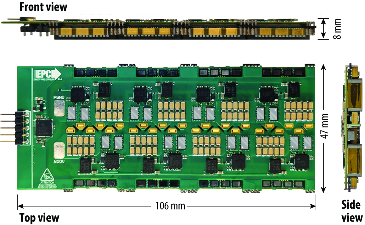
Figure 3: EPC91123 – 6 kW 800 V to 12.5 V ISOP GaN Converter Evaluation Board
Robotics: Compact Power Enables Motion Intelligence
Robotics represents one of the most structurally important long-term growth drivers for gallium nitride technology. Unlike stationary infrastructure platforms, mobile robotic systems impose strict constraints on weight, volume, and energy efficiency.
Each actuator (e.g. motor drive) inside a humanoid robot contains a localized power conversion stage, and the aggregate impact across dozens of joints becomes decisive for system autonomy.
As Alex Lidow observed:
“A humanoid robot has about 40 actuators, and GaN devices can make those actuators not just more efficient but about one-tenth the volume.”
This reduction is not incremental. It directly affects battery lifetime, thermal management, and mechanical integration strategies. The same architectural advantages extend to surgical robotics and advanced prosthetic platforms, where compact motor-drive electronics improve motion precision and responsiveness.
As robotics platforms evolve toward higher dexterity and longer operating cycles, switching technologies capable of delivering both efficiency and miniaturization simultaneously - such as GaN - are becoming foundational rather than optional components of actuator design.
Figure 4: Motor Control Solutions for Humanoid
Silicon Carbide and GaN: Complementary, Not Competitive
Gallium nitride isn’t the only wide-bandgap semiconductor transforming power electronics. Silicon carbide is on a similar adoption curve – but at higher voltage levels.
As Lidow summed up: “Above about 650 volts, silicon carbide is a better solution.
This difference indicates a structural difference between the two materials. Gallium Nitride devices are generally lateral and thus very efficient in sub-650 V architectures, while silicon carbide is more appropriate for vertical conduction structures more suited to traction inverters and high-voltage conversion systems.
Rather than competing directly, the two technologies are delineating complementary operating domains across electrified infrastructure.
GaN is enabling small high-frequency switching stages in intermediate bus architectures, robotics platforms and AI power delivery networks.
In contrast, silicon carbide is increasingly used in place of IGBTs for high-power automotive traction systems and grid-level conversion equipment.
Combined they are the foundation for the next generation of wide bandgap power electronics.
e-mobility
Both gallium nitride (GaN) and silicon carbide (SiC) will play important but different roles in e-mobility. Modern EVs also have an increasing number of auxiliary loads that were once driven mechanically, such as air-conditioning compressors, pumps and other accessories that were once belt-driven from the engine. The functions are being electrified today and are increasingly standardized on a 48 V bus in today’s electric platforms.
Lidow says, “That’s really where GaN shines, in the 48 V domain.” EPC has specifically optimized its GaN devices for 48 V applications, and he argues that for 48 V power stages you simply can't beat GaN for efficiency, power density and size. So SiC will dominate high-voltage traction drives in EVs, and GaN will take an increasing share of the 48 V auxiliary and power-conversion subsystems.
The Remaining Bottleneck: Magnetics
One of the most important constraints in next-generation power conversion is no longer the semiconductor itself - but the passive components surrounding it.
As switching frequencies move from hundreds of kilohertz toward the MHz domain, traditional magnetic components are becoming the limiting factor in converter scaling. As Lidow noted:
“Magnetics were designed for hundreds of kilohertz. With GaN people want to go megahertz.”
Higher switching frequency enables smaller inductors, reduced capacitance requirements, faster transient response, and significantly higher power density. However, without parallel advances in magnetic materials and packaging techniques, system designers cannot fully exploit GaN’s performance envelope.
For the passive-component ecosystem, this represents not a limitation - but a major innovation opportunity.
Looking Beyond GaN: Future Wide-Bandgap Materials
Several emerging materials - including gallium oxide, aluminum nitride, and diamond - are attracting attention as potential next-generation wide-bandgap platforms.
Their theoretical performance limits are impressive, particularly for ultra-high-voltage applications. However, material capability alone is not sufficient to drive adoption. Manufacturing infrastructure and system-level relevance remain decisive factors.
As Lidow observed: “You still need a killer application before a new semiconductor technology becomes broadly useful.”
For now, gallium nitride remains far from its own theoretical limits. With strong compatibility with silicon manufacturing infrastructure and expanding deployment across AI, robotics, and space systems, GaN still has a long innovation runway ahead.
A Message to the Next Generation of Engineers
Technology shifts favor engineers who foresee change, not the ones who chase it. Lidow concluded:
“Don’t go with the popular choice today. Chase the future.”
That’s the kind of opportunity gallium nitride presents. Wide-bandgap power conversion is reshaping energy processing across modern systems, from AI infrastructure and robotics to aerospace electronics and distributed electrification platforms.
The message to the new engineers entering the field today is clear: the next wave of impact will not come from incremental optimization, but from choosing the technologies that enable totally new architectures.