eGaN FET 是低 EMI 解決方案!
技術分享雜談GaN技術 – Michael de Rooij, Ph.D.
五月 19, 2020
GaN FETs 可以比 Si MOSFETs 切換得更快,這使得許多系統設計師會問−更快的切換速度如何影響 EMI?
本博客討論了在使用 eGaN® FETs 設計切換轉換器系統時考慮的簡單緩解技術,並將展示為什麼 GaN FETs 產生的 EMI 比 MOSFETs 少,儘管其切換速度很快。
EMI 系統概述
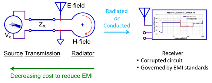 圖 1:EMI 系統概述
圖 1 顯示了 EMI 系統的組成部分:
EMI 系統的第一個組成部分是能量源,這可以以不同形式產生,例如晶體管的切換事件。來自能量源的能量需要傳輸路徑,例如在PCB上的導體。這些傳輸路徑可以形成電容器的極板,電壓可以作為 E 場輻射,或者在電流路徑形成的迴路中,電流可以作為 H 場輻射。同樣可能的是,一個迴路可以輻射 E 場,反之亦然,電容器的極板可以輻射 H 場。
無論傳輸方式和路徑如何,EMI 能量必須被接收。在直接傳輸的情況下,稱為“傳導 EMI”,在場的情況下,稱為“輻射”。
EMI 系統的最後一個組成部分是接收器,根據定義,這是一個電路,由於 EMI 受到污染,導致不希望的行為。接收電路可以是包含能量源的同一電路,也可以是第三方電路,例如收音機接收器。在第三方接收器電路的情況下,防止 EMI 誘發的不希望行為由 EMI 標準管理。
為合規和防止污染而採取的 EMI 緩解措施不可避免地增加了系統成本。越接近(並包括)能量源採取措施處理 EMI,系統成本越低。
佈局的影響
佈局是一種零成本的 EMI 緩解措施。在設計轉換器時,佈局本身具有寄生電感。在圖 2 所示的同步降壓轉換器示例中,顯示了在上升沿硬切換轉換後,迴路電感對開關節點電壓過衝的影響。
左側圖像顯示了具有約 1 nH 迴路電感的佈局,結果是 70% 峰值電壓過衝和振鈴。右側圖像顯示了具有 400 pH 迴路電感的佈局,結果是 30% 峰值電壓過衝和振鈴。
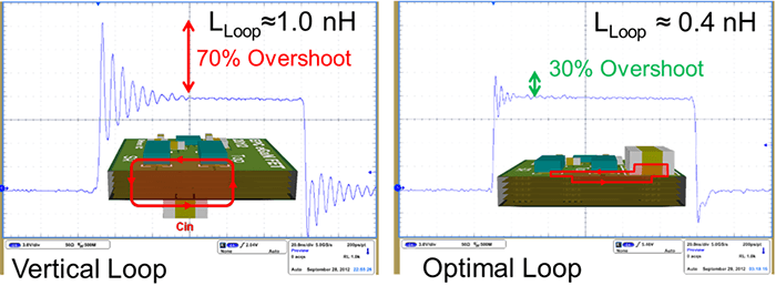 圖 2:佈局對過衝的影響
生成的 EMI 與電壓過衝幅度的平方成正比,通常以 E 場形式從形成電容器的導體發射。迴路電感在振鈴期間也會導電流,生成的 EMI 與電流幅度的平方成正比,通常以 H 場形式從電源迴路電路發射。
將電源迴路電感減半可以使生成的 EMI 減少四倍。
上升/下降時間的影響
儘管 GaN FETs 可以比 MOSFETs 切換得更快,但重要的是要注意,僅僅因為一個器件切換得比另一個更快,EMI 能量基本上不會改變。僅僅是頻譜內容的變化。
這在圖 3 的示例中顯示,該示例使用 1 MHz 操作的降壓轉換器,將 48 V 輸入電壓轉換為 12 V,分別針對 5 ns 和 1 ns 的兩個切換瞬態條件。該圖顯示了兩種瞬態條件下開關節點電壓的頻譜,上升沿時間設置為與下降沿時間相同,並且不包括電壓過衝和振鈴。
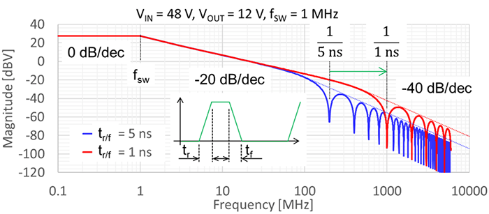 圖 3:上升/下降時間對頻譜內容的影響
在 90 MHz 時,頻譜內容已經衰減了 42 dB。在 5 ns 瞬態情況下,第一個顯著頻率是 200 MHz,即 1/5 ns;在 1 ns 瞬態情況下,第一個顯著頻率是 1 GHz,即 1/1 ns。
上述這些頻率的頻譜幅度下降率為每十年 40 dB,這意味著過濾要求已經非常低,因此使得處理前面討論的電壓過衝振鈴更加重要。
開關節點實際上形成了與地面成對的電容板,這種形式的 EMI 以 E 場輻射為主。
反向恢復的影響 (QRR)
最後,作為一個示例,評估了在硬切換降壓轉換器中反向恢復對 EMI 的影響,這通常被忽視。
反向恢復表現為電源迴路中的貫穿電流,正如前面討論的那樣,電源迴路中的電流會導致電壓過衝和振鈴。反向恢復會增加電源迴路中的能量,從而增加 EMI 噪聲源的能量,這與反向恢復電流的平方成正比。這個反向恢復電流的幅度可能比降壓轉換器的電感電流高出幾倍。
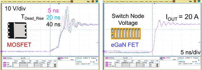 圖 4:反向恢復的影響 (QRR)
圖 4 左側波形顯示了 MOSFET 基於的降壓轉換器在分別為 5 ns、20 ns 和 40 ns 的死時間條件下的電壓過衝和振鈴,而右側波形顯示了在相同操作條件下的 eGaN FET 等效情況。
可以在右側波形看到,死時間的變化對 eGaN FET 沒有影響,因為它具有零反向恢復。
摘要
eGaN FETs 和 ICs 具有 EMI 兼容性。通過採用簡單的佈局技術,可以確保顯著減少 EMI 產生,而不會增加 EMI 緩解成本。
更高的切換速率僅會導致頻譜內容的變化,但不會增加 EMI 能量。在更高頻率下,EMI 減少技術更有效,從而降低實施成本。
最後,eGaN FETs 和 ICs 以晶圓級芯片封裝(WLCS)形式提供,具有幾乎為零的內部電感,並且具有零反向恢復,因此在硬切換轉換器中本質上會產生更少的 EMI 能量。
儘管其切換速度顯著更快,eGaN FETs 產生的 EMI 比 MOSFETs 更少。
注意:欲了解更多信息,包括 Würth Elektronik 對電感選擇和放置影響的詳細討論,請參閱我們的 How to GaN 系列視頻:設計基礎:EMI 緩解技術。