EPC9048C:開発基板

EPC9048C: 200 V, 15 Aのハーフブリッジ開発基板

EPC9048Cの開発基板

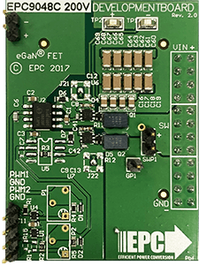
開発基板EPC9048Cは、エンハンスメント・モード(eGaN®)電界効果トランジスタ(FET)のEPC2034Cを搭載し、最大デバイス電圧200 V、最大出力電流15 Aでゲート駆動回路を搭載したハーフブリッジです。

The EPC9092 development board is 1.5” x 2” and contains two EPC2034C eGaN FETs in a half bridge configuration. The gate driver used on this board is ON Semi’s NCP51820.

To simplify the evaluation process of theEPC2034CGaN FET, all the critical components and layout for optimal switching performance are implemented. ビデオ:EPCの開発基板をプロトタイプに変える方法

ステータス:廃止
GaNのエキスパートたちは、新しい設計に EPC9099を提案しています。
Ask and EPC Engineer a Question FAQ

EPCのeGaN FETと
ICについて質問が
ありますか?
GaNエキスパートに聞く

EPC9048C Parameters Table
(1) Maximum input voltage depends on inductive loading, maximum switch node ringing must be kept under 200 V for EPC2034C.
(2) Maximum current depends on die temperature – actual maximum current is affected by switching frequency, bus voltage and thermal cooling.
(3) When using the on board logic buffers, refer to the NCP51820 datasheet when bypassing the logic buffers.
(4) Limited by time needed to ‘refresh’ high side bootstrap supply voltage.