客戶可以在我們的網頁 註冊 ,定期收取最新消息包括全新產品發佈、應用文章及更多其它資訊。如果你錯過了已發佈的消息,你可瀏覽以下的文檔。
根據將氮化鎵和碳化矽材料的電子從價帶轉移到導帶所需的能量,氮化鎵和碳化矽元件被指定爲寬帶隙 (WBG) 半導體——碳化矽元件約爲 3.2 eV,氮化鎵元件則約爲 3.4 eV,而矽元件只有1.1 eV 。WBG 的擊穿電壓更高,在某些應用中可以達到 1,700 V。 在今年 5 月舉行的綫上PCIM Europe展會上,幾家公司展示了他們在 氮化鎵和碳化矽技術方面的最新創新,並且就 WBG 技術的發展方向分享了其獨特見解。
EE Times – Europe
2021 年 7 月
閱讀文章
閱讀全文
航太應用的技術發展是 2021 年的重要組成部份,因此更多的抗輻射元件即將問世。 最近新推兩款新型場效應電晶體,它們給航太領域帶來了甚麽?
All About Circuits
2021 年 6 月
閱讀文章
閱讀全文
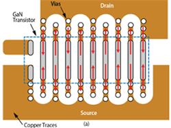
氮化鎵電晶體和積體電路提高了馬達控制應用的功率密度。最佳佈局允許從橋臂分流器或同相分流器獲得沒有振鈴噪聲的輸出開關波形和“乾淨“的電流重建信號。
Bodo’s Power Systems
2021 年 6 月
閱讀文章
閱讀全文
(Image: Yole)
Posted 2021年5月10日
Manufacturers of GaN power semiconductors showcased their latest products, from 100 V to 650-V devices at PCIM Europe. PCIM Europe showcased several presentations about the benefits and use cases of wide bandgap (WGG) semiconductors, including gallium nitride (GaN) and silicon carbide (SiC). Several manufacturers, including EPC, GaN Systems, Infineon, Nexperia, and STMicroelectronics announced several new families of GaN power semiconductors during the week.
Electronic Products
May, 2021
Read article
閱讀全文
最近,EPC公司對其氮化鎵場效應電晶體(eGaN FET)進行了一系列測試,把它置於超出數據手冊的限值下工作,從而量化和發表這些元件通過電壓和電流極端應力測試的結果。
Bodo’s Power Systems
2021年5月
閱讀文章
閱讀全文
In this article, the author introduces a GaN FET compatible analog controller that yields a low bill-of-material count and give designers the ability to design a synchronous buck converter in the same simple way as using silicon FETs, and offers superior performance for 48 V power systems.
Power Electronics News
April, 2021
Read article
閱讀全文
氮化鎵電晶體和積體電路通過消除輸入濾波器中的電解電容,以提高馬達控制應用的功率密度。氮化鎵元件的卓越開關性能可消除死區時間且實現無與倫比的正弦電壓和電流波形,從而實現更平滑且沒有雜訊的操作。
Bodo’s Power Systems
2021年4月
閱讀文章
閱讀全文
氮化鎵技術發展迅速,在開發出多代全新離散元件後,具備更高效、更小尺寸和成本更低等優勢的新世代積體電路繼續崛起。氮化鎵積體電路讓產品可以更小型化、開關更快、更高效且更易於設計。
Power Systems Design
2021年3月 (第36-39頁)
閱讀文章
閱讀全文
Gallium nitride (GaN) power devices have been in production for over 10 years and, beyond just performance and cost improvements, the most significant opportunity for GaN technology to impact the power conversion market comes from the intrinsic ability to integrate multiple devices on the same substrate. This capability will allow monolithic power systems to be designed on a single chip in a more straightforward, higher efficiency, and more cost-effective way.
Power Electronic News
March, 2021
Read article
閱讀全文
New family of laser driver IC products will enable faster adoption and increased ubiquity of ToF solutions across a wider array of end-user applications.
How2Power
March, 2021
Read article
閱讀全文
Enhancement-mode gallium nitride (eGaN) FETs have demonstrated excellent thermomechanical reliability in actual operation in the field or when tested according to AEC or JEDEC standards. This is because of the inherent simplicity of the “package,” the lack of wire bonds, dissimilar materials, or mold compound. Recently, an extensive study of underfill products was conducted to experimentally generate lifetime predictions. A finite element analysis at the end of this section explains the experimental results and generates guidelines for selection of underfill based on key material properties.
Bodo's Power
March, 2021
Read article
閱讀全文
In last month’s Safety & Compliance column in How2Power, “WBG Semiconductors Pose Safety And EMI Challenges In Motor Drive Applications,”[1]Kevin Parmenter made some assertions about the difficulties of using SiC, and to a lesser extent GaN, power semiconductors in large motor-drive applications. This commentary is a response to that article, showing that GaN can be a game changer in low-voltage integrated motors.
How2Power
February, 2021
Read article
閱讀全文
Gallium nitride (GaN) devices offer performance in a small form factor, increasing the efficiency, and reducing the system cost for 48 V power conversion applications. They have been adopted in high volumes in high density computing, as well as many new automotive power system designs.
Electronic Specifier
February, 2021
Read article
閱讀全文
This article discusses the challenges that thermal management raises due to increase power density, especially with chip-scale packaging (CSP). What is sometimes overlooked, however, is that CSP eGaN® power FETs and integrated circuits have excellent thermal performance when mounted on standard printed circuit board (PCBs) with simple methods for attaching heat sinks. Simulations, supported by experimental verification, examine the effect of various parameters and heat flow paths to provide guidance on designing for performance versus cost.
Bodo’s Power Systems
February, 2021
Read article
閱讀全文
This article discusses how GaN-based solutions coupled with digital control increase efficiency, shrink the size, and reduce system costs for high density computing applications like ultra-thin laptops and high-end gaming systems. As computers, displays, smartphones and other consumer electronics systems become thinner and more powerful over the past decade, there is increasing demand for addressing the challenge of thinner solutions while extracting more power out of limited space. To address this challenge, the comparative advantages of various non-isolated DC-DC step-down topologies for ultra-thin 48 V – 20 V power solutions that are designed to fit inside a notebook computer or an ultra-thin display are examined.
Power Electronics News
January, 2021
Read article
閱讀全文
Gallium nitride (GaN) transistors have been in mass production for over 10 years. In their first few years of availability, the fast switching speed of the new devices – up to 10 times faster than the venerable Si MOSFET – was the main reason for designers to use GaN FETs. As the pricing of GaN devices normalized with the MOSFET, coupled with the expansion of a broad range of devices with different voltage ratings and power handling capabilities, much wider acceptance was realized in mainstream applications such as DC-DC converters for computers, motor drives for robots, and e-mobility bikes and scooters. The experience gained from the early adopters has led the way for later entrants into the GaN world get into production faster. This article is the first in a series of articles discussing three topics that can help power systems designers achieve the most out of their GaN-based designs at the lowest cost. The three topics are: (1) layout considerations; (2) thermal design for maximum power handling; and, (3) EMI reduction techniques for lowest cost.
Bodo’s Power Systems
January, 2021
Read article
閱讀全文
Standard qualification testing for semiconductors typically involves stressing devices at-or-near the limits specified in their data sheets for a prolonged period of time, or for a certain number of cycles. The goal of qualification testing is to have zero failures out of a large group of parts tested. By testing parts to the point of failure, an understanding of the amount of margin between the data sheet limits can be developed, but more importantly, an understanding of the intrinsic failure mechanisms of the semiconductor can be found.
IEEE Power Electronics Magazine
December, 2020
Read article
閱讀全文
An automotive application using GaN power devices in high volume is lidar(light detection and ranging) for autonomous vehicles. Lidar technology provides information about a vehicle’s surroundings, thus requiring high accuracy and reliability to ensure safety and performance. This article will discus a novel testing mechanism developed by EPC to test eGaN devices beyond the qualification requirements of the Automotive Electronics Council (AEC) for the specific use case of lidar.
Power Systems Design
December, 2020
Read article
閱讀全文
Gallium nitride power device technology enables a new generation of power converters in space operating at higher frequencies, higher efficiencies, and greater power densities than everachievable before. GaN power devices can also exhibit superior radiation tolerance compared with Silicon MOSFETs depending upon their device design.
Power Electronics Europe
December, 2020
Read article
閱讀全文
氮化鎵(GaN)技術已實現重大改進,而且它極具成本效益,可以替代MOSFET元件。 從2017年開始,採用氮化鎵元件的48 V DC/D轉換器開始成為市場上重要的應用。 各種拓撲諸如多相和多級降壓轉換器,實現具備更高效率的全新解決方案,可以滿足IT和汽車市場的能源需求。
Power Electronics News
2020年11月
閱讀全文
閱讀全文