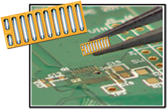
 The EPC “How to GaN” educational series is designed to accelerate your learning curve for gallium nitride technology. Theory and real world application of high performance GaN power transistors are explored.
Modules available:
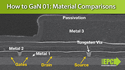 How to GaN 01 – Material Comparisons
This video will provide a basic understanding of why gallium nitride is such a great semiconductor material and how its capabilities are enabling power conversion designers to reduce power losses, reduce system size, improve efficiency, and ultimately, reduce system costs.
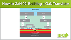 How to GaN 02 – Building a GaN Transistor
This video will provide a basic understanding of how to build a GaN transistor utilizing a low cost substrate and a large, well-developed infrastructure.
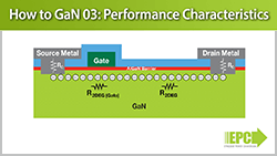 How to GaN 03 – Performance Characteristics
In this video, the basic physical properties of GaN transistors will be correlated to the electrical characteristics that are important when developing power conversion circuits and systems.
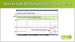 How to GaN 04 – Design Basics: Gate Drive
In this video, the basic techniques for using GaN transistors in high-performance power conversion circuits is discussed. GaN transistors generally behave like power MOSFETs, but at much higher switching speeds and power densities. This video will focus on how to drive a GaN transistor to achieve maximum performance.
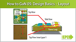 How to GaN 05 – Design Basics: Layout
In this video, the basic layout techniques for using GaN transistors to achieve maximum performance in high-performance power conversion circuits is discussed.
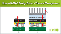 How to GaN 06 – Design Basics: Thermal Management
In this video, the thermal design for GaN transistors is discussed. Thermal design becomes increasingly critical with the latest generation of GaN transistors, where smaller die sizes and chip-scale packages are harnessed to improve electrical performance. This video will show how heat extraction from a small GaN transistor or integrated circuit, with a good thermal design, can be as effective as from a bulky silicon MOSFET.
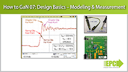 How to GaN 07 – Design Basics: Modeling and Measurement
In this video, the measurement and modeling of GaN transistors for predicting actual in-circuit behavior is discussed.
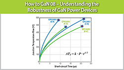 How to GaN 08 – Understanding the Robustness of GaN Power Devices
This video will detail the critical aspects GaN power device reliability and show how testing gallium nitride devices to failure demonstrates robustness unmatched by silicon power MOSFETs.
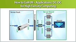 How to GaN 09 – Applications: DC-DC for High Density Computing
In this video, the advantage of GaN-based solutions for high density computing applications is discussed. Advanced computing applications for cloud computing, artificial intelligence, machine learning, and multi-user gaming are putting higher demands on power converters to deliver much more power in smaller form factors. Due to the significant performance improvements that GaN offers, a fundamental shift in the server architecture is possible that significantly increases efficiency, shrinks size, and reduces system cost.
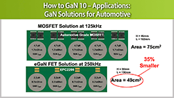 How to GaN 10 – Applications: GaN Solutions for Automotive
In this video, application examples where GaN technology and devices are improving automotive systems are presented. GaN devices are AEC Q101 qualified and offer improved performance over the aging silicon MOSFET used in vehicles today, enabling higher efficiency and high reliability with densities higher than ever achievable before. This enables systems that are smaller, more efficient, and lower cost.
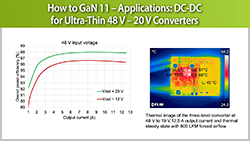 How to GaN 11 – Applications: DC-DC for Ultra-Thin 48 V – 20 V Converters
In this video, showing how leveraging the advantages of eGaN FETs, such as small size and low losses, enhances the performance of ultra-thin, multilevel converters is discussed. Since GaN transistors are smaller and faster than MOSFETs, and offer a significant reduction in board real estate, multilevel topologies have become attractive as a solution to meet the demands by computers, displays, smart phones, and other consumer electronic systems to design thinner solutions while extracting more power out of limited space.
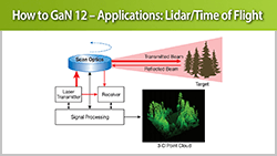 How to GaN 12 – Applications: Lidar/Time of Flight
In this video, time-of-flight lidar applications are discussed. Although lidar systems have been in use for decades, until recently they have been expensive and bulky. The high performance of GaN transistors has been a key factor in the development of modern, cost‐effective lidar systems by enabling laser drivers with extremely fast, high current pulses.
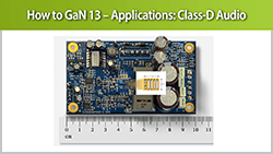 How to GaN 13 – Applications: Class-D Audio
In this video, GaN-based Class-D audio amplifier applications are discussed. GaN-based class-D audio provides better sound quality in smaller form factors that can be built at a lower cost.
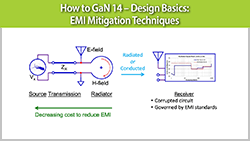 How to GaN 14 – Design Basics: EMI Mitigation Techniques
In this video, EMI mitigation techniques for consideration when designing switching converter systems using eGaN FETs and ICs including passive components is discussed. The video starts with an overview of an EMI system and then discusses the effects of specific design choices on EMI generation such as layout, rise/fall times and reverse recovery. Lastly, Würth Elektronik’s presents the impact of inductor choice and placement on EMI propagation and mitigation.