4.2 Enhance Your Design with Our Recommended Layout Strategies
GaN transistors generally behave like power MOSFETs, but at much higher switching speeds and power densities, therefore layout considerations are very important and care must be taken to minimize layout parasitic inductances.
The recommended design for Optimizing PCB Layout with eGaN FETs (WP010) utilizes the first inner layer as a power loop return path. This return path is located directly beneath the top layer’s power loop allowing for the smallest physical loop size. Variations of this concept can be implemented by placing the bus capacitors either next to the high-side device, next to the low-side device, or between the low and high-side devices, but in all cases, the loop is closed in the inner layer right beneath the devices. A similar concept is also used for the gate loop, with the return gate loop located directly under the ON and OFF gate resistors.
Furthermore, to minimize the common source inductance between power and gate loops, the power and gate loops are laid out perpendicular to each other, and a via next to the source pad closest to the gate pad is used as Kelvin connection for the gate driver return path.
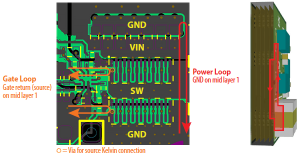 Inner Vertical Layout for Power and Gate Loops
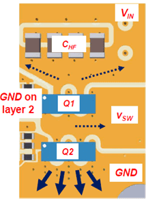 Top Cap Layout
- GND return in mid-layer 1 → no vias allowed in Q1(HS) Drain
- GND plane connected to Q2(LS) → best thermals for LS
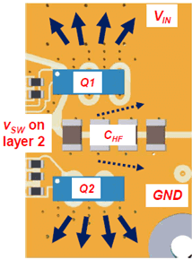 Middle Cap Layout
- VIN plane connected to Q1(HS) and GND plane connected to Q2(LS) on top layer
- Full vias and more spread out devices → best thermal performance for LS and HS
- Buried switch node
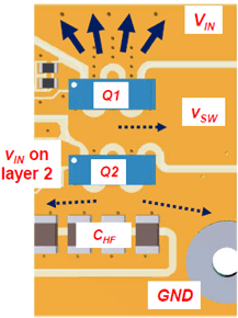 Bottom Cap Layout
- VIN return in mid-layer 1 → no vias allowed in Q2(LS) Source
- VIN plane connected to Q1(HS) → best thermals for HS
Additional Resources
4.3 Guidelines for Effective Parallelling of Devices
For higher-power applications, it may be necessary to place multiple transistors in parallel and have them behave as a single device. GaN devices parallel extremely well because:
- The RDS(ON) has a positive temperature coefficient, so in the ON-state the current will self-balance based on each device temperature
- The QG of GaN FET is much lower than comparable Si MOSFET, therefore the requirements and the losses in the gate driver are minimized
- The VTH of GaN FET is very stable over temperature, as compared to a strongly negative temperature coefficient for Si MOSFET, this allows good current sharing also during switching events
However, to ensure good current sharing in dynamic conditions, it is also important to pay attention to the layout:
- Individual gate resistors should be used for each GaN FET, placed near the FETs
- All parasitic inductances in the layout should be kept as similar as possible for each paralleled device, both for the power loop and gate loop
- For high-performance applications, we recommend a layout technique of paralleling half-bridges instead of single devices: Paralleling High Speed GaN Transistors (AN020).
An example of a parallel layout with 4 devices in parallel is the EPC90135: 100 V, 45 A Parallel Evaluation Board
Many EPC parts are offered in a Wafer Level Chip Scale Package (WLCSP) using a fine pitch down to 400 µm. This means a proper PCB footprint design is essential for consistent and reliable assembly of the GaN device. Detailed recommendations can be found here How2AppNote008 - Designing PCB Footprint eGaN FETs ICs, and recommended land patterns (solder mask opening) and stencil designs are provided in each datasheet. EPC also provides an Altium Library with all the EPC footprints. The video Footprint Design – PCB CAD System Independent guides customers through a CAD-independent detailed explanation of how to create their own footprints.
EPC recommends the use of a Solder Mask Defined (SMD) pad over a Non-Solder Mask Defined (NSMD) pad for two reasons:
- A Solder Mask Defined (SMD) footprint yields lower inductance and improves alignment during reflow.
- A Non-Solder Mask Defined (NSMD) footprint has a higher probability of die misalignment during reflow, which can reduce the effective copper contact area thereby degrading the solder joint and current carrying capability of the device.
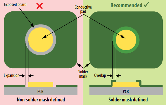 Solder mask defined versus non-solder mask-defined pad
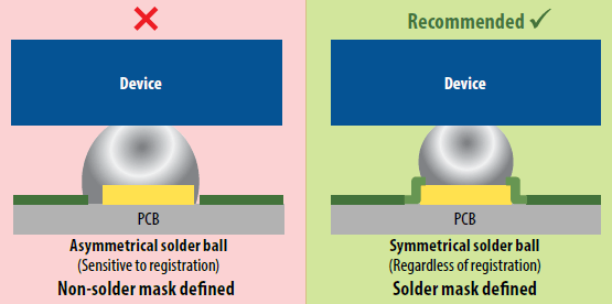 Effect on the solder ball symmetry
EPC recommended silkscreen design should include:
- 4 corner registration marks outlining the part shape.
- Lines drawn with an open narrow dash: a solid line rectangle surrounding the part, thus preventing flux from flowing away from the die during the reflow process, can create a flux dam and trap flux under the part.
- Unique Pin one identifier.
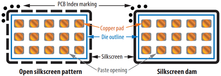 Differences between open silkscreen pattern and silkscreen dam
If you would like the EPC team to review your design once the schematic and layout are done, please submit request to [email protected]