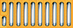
 Figure 1: Mounting side of EPC2001 [2]The ultra high speed switching capabilities of eGaN FETs enable a new state-of-the-art in power density. Realizing the high switching speeds that they are capable of requires minimal inductance to reduce dynamic losses and ringing. Old school packaging ideology would not allow this. EPC’s innovative wafer level, Land Grid Array (LGA) packaging enables high frequency loop inductance of a half bridge circuit to be demonstrated as low as 400 pH, which allows overshoot of just 23%, minimal ringing, and a 2.5% efficiency gain compared with a 1.6 nH layout at 12 V, 1 MHz [1]. Figure 1 shows a photograph of the mounting side of an EPC2001 which has a land pitch of 0.4 mm.
While fine pitch packages have been used in high volume production in small signal applications, their use will be a learning opportunity to many power engineers.
Overview
For a reliable, high yielding assembly, LGA eGaN FETs must:
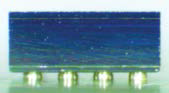
Figure 2: Properly mounted device
- Have all flux rinsed from between lands and be dry before applying power.
- Be assembled level to the board with enough standoff to rinse any flux from between the lands.
- Have the correct solder volume and reflow process to provide sufficient height for proper rinsing of any solder flux from between the lands, but not excessive solder, where the joint becomes unstable and tilts or collapses during reflow.
- Have the correct PCB solder mask footprint for each solder bump to ensure proper contain-ment of solder.
- Use underfill if the assembly will be exposed to moisture during use.
Figure 2 shows a side view of a properly mounted device.
Land Design and PCB Traces
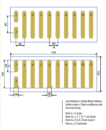 Figure 3: Recommended Land Pattern for EPC2001
The LGA footprint is solder mask defined. This means that the copper trace is larger than the solder mask opening in all directions, bounding the solder flow by the solder mask. Solder mask openings should be slightly smaller than the corresponding solder bump. Recommended land patterns for each device are provided on their datasheet. The recommended land pattern for the EPC2001 is shown in Figure 3. Oversized solder mask open-ings can lead to solder bridging from land to land in the short direction, too narrow of a channel for sufficient rinsing, or die tilt in the long direction. Undersized openings lead to solder overflowing the solder mask causing shorts or die tilt. This is especially critical for small bumps when larger bumps are also present on the die. Boards should be checked against drawing as they sometimes don’t match. Typical solder mask thickness should not exceed 25 µm (1 mil).
While the eGaN FET LGA package is quite small, it must still be remembered that these devices are designed to carry significant current. Two ounce copper has been used successfully and has good electrical and thermal characteristics. Heavier copper traces may become too narrow for the 0.4 mm pitch of some of EPC’s devices while lighter traces will sacrifice thermal and electrical performance.
Vias should not be placed in the lands unless they are completely filled. Unfilled vias will wick solder away from the joint and may cause die tilt or insufficient standoff for proper cleaning.
Solder Volume and Stencil Design
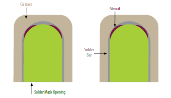 Figure 4: Top view showing the relationship between the solder bar, solder stencil, and top copper trace.
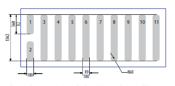 Figure 5: Recommended Laser Cut Stencil Aperture Design for EPC2001 (units in µm)
Correct solder volume will help ensure a proper assembly and allow proper cleaning of the device. For type 3 solder, reflowed solder volume from the paste should be roughly equal to the solder volume on each terminal, above the solder mask. Care must be taken to account for the metal load of the solder when determining the solder volume and hence, the solder mask and stencil opening areas. The PCB footprint is solder mask defined where the solder area is defined by the solder mask opening. The volume will be based on stencil thickness. A 100 µm thick stencil is recommended.
Type 4 solder has smaller particles, and flows more freely leading to a higher risk of die tilt and solder bridging. If type 4 solder must be used, less solder is required (Please consult with EPC about stencil designs for type 4 solder. Contact us by e-mail at [email protected]). For example, the 180 µm wide stencil opening for the EPC2001 should be re-duced to 165 µm (6.5 mils) for type 4 solder.
For a 100 µm stencil, type 3 solder, 88.5% metal loading, the stencil opening should be the same size as the solder mask opening with the corners of the apertures rounded to a radius of 60 µm. The recommended stencil design for the ends of two bars of the EPC2001 is shown in figure 4.
Laser cut stencils have a straighter wall than chemically etched stencils. A laser cut stencil will, in general, result in more solder volume released than a chemically etched stencil of the same aperture. The 180 µm wide stencil aperture is recommended for a laser cut stencil. A slight adjustment wider (up to 200 µm (7.9 mils) wide) might be required for chemically etched stencils to obtain sufficient solder volume release. The recommended solder stencil for the EPC2001 under the recommended conditions is shown in figure 5.
For variations of stencil thickness, solder type or metal fill, or stencil type, EPC should be consulted about stencil design. E-mail [email protected].
Reflow
The reflow profile should be according to solder manufacturer instructions. The reflow profile must be adjusted depending on board size, the thermal mass of components, the oven type as well as other reflow conditions. If LGA packages are mounted near large, thermally massive components or copper areas, tests must be conducted to make sure the LGA packages’ solder flows completely and evenly so the devices do not tilt. For reference, profiles are given for AIM Solder NC257-2 SAC305 Lead Free, No Clean Solder Paste in figure 6 [3]. Note that AIM refers to these as “starting points” for solder profile adjustment. Vibrations in the reflow oven may cause the solder to become unstable and collapse causing die tilt or solder bridging. Uneven heating can also result in tilt.
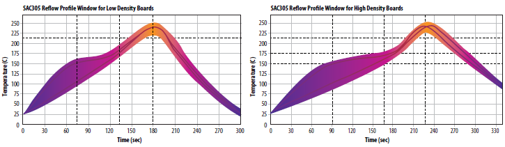
Figure 6 – AIM Solder NC257-2 SAC305 solder reflow profile guideline “starting points”
Rinsing
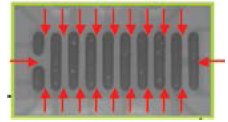 Figure 7: X-Ray of eGaN FET after assembly showing rinse direction recommendations
As with any fine pitch assembly, solder manufacturers recommend that residual flux is rinsed using the manufacturers recommended solvent. They recommend this even with “no rinse” flux because residual flux combined with the electric field of the fine pitched devices create conditions under which dendrites can grow rapidly. Boards should be rinsed in all four directions to ensure removal of residue from all areas under the die as shown in figure 7. After rinsing, the assemblies should be dried according to the solvent manufacturer’s instructions as the solvent can also facilitate dendrite growth. In general, deionized water should not be used as a rinse for no rinse flux as it combines with the flux to form a residue where dendrites can grow.
Underfill
Underfill should be used in applications where the board is exposed to moisture. Moisture and other contaminants may provide an environment which allows dendrite growth. The underfill materials used successfully by EPC up to 125°C were Loctite Hysol FP4549Si [4] and Shin-Etsu SMC375X7 [5].
Component Attach After Reflow
In the case where flux is used to attach additional components after attachment of the eGaN FETs, flux from this later operation may flow between the LGA lands providing an environment for dendrite growth. This can be prevented by the use of underfill; or the flux can be removed by rinsing in all direction in accordance with the flux or solder manufacturer’s instructions. As post-re-flow soldering is often done by hand, the amount of flux is not well controlled. Proper training of the operator to use minimal flux is important because there is an urge to use excessive flux for easy soldering. It is advised to bake the board to cure any leftover flux. Flux can generally be cured by baking the board at 150° C for 30 minutes or 125° C for 60 minutes. These are minimum times for the board to remain at these temperatures. In the event of massive amounts of flux getting between the lands, it might not be removed or cured after rinse and/or bake.
Design Example
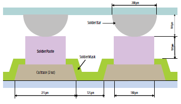 Figure 8: Cross section of an example PCB Mount using EPC2001 (Pre-reflow) Per solder mask defined, there is no gap between the solder mask and Cu trace
Figure 8 is a drawing of a cross section of an EPC2001 on the NC257-2 SAC305 Lead Free, No Clean Solder Paste mounted on the PCB with a two ounce copper top side metal layer. We will use the cross sectional area as proxy for solder volume. Per the datasheet, the solder bump radius is 100 µm giving a cross sectional area of 15.7 nm2. Using NC257-2 SAC305 lead free, no clean, type 3 solder paste with an 88.5% metal load, and 100 µm stencil thickness, the solder mask width comes to approximately 180 µm.
Inspection
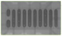 Figure 9: X-Ray of EPC2001 after solder stencil assembly process
eGaN FETs are mechanically robust and have demonstrated high yield in volume assembly. Damage, however, can still occur if several standard precautions are not taken to ensure adequate solder reflow, reduce excessive die tilt, and avoid residual uncured solder flux.
Even though eGaN FETs have been designed such that the reflowed solder is visible to the unaided eye, the best way to determine if devices have been properly reflowed is by producing X-ray images. Figure 9 shows an X-ray image of an EPC2001 assembled with a solder stencil process. As can be seen, minimal voiding is present giving highly reliability and excellent thermal and electrical characteristics.
Dendrites
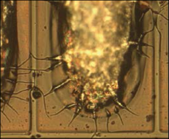 Figure 10: eGaN FET showing dendrite formation after exposure to residual flux
Incomplete cleaning and drying can leave uncured flux, which is a medium in which dendrites can grow. Figure 10 shows dendrites shorting two terminals in uncured flux.
Die Tilt
A tilted die will make the device impossible to thoroughly clean, leaving residual flux and enabling dendrite growth. Figure 11 shows a tilted die. The main causes of die tilt were found to be; (1) uneven thickness of solder paste, (2) excessive vibration during reflow, (3) non-optimized temperature profile and (4) oversized solder mask and / or oversized solder stencil (too high solder volume). Normally, the solder flows evenly and melts roughly at the same time. Care must be taken to adjust the solder reflow profile when an element of significant mass is located nearby. All of the solder has to flow for the surface tension to level and align the device.
 Figure 11: End view of a tilted die with trapped flux
Solder Bridging
Solder bridging can occur due to excessive solder volume or undersized solder mask opening, particularly where bump lengths vary within a die such as the gate and substrate bumps of the EPC2001. The excess volume does not have enough surface tension to hold the solder together, and the solder collapses, shorting one terminal to another. Too wide of a solder mask opening can reduce the distance between the solder between bars and make it easier to short.
Summary
LGA packages provide the low inductance necessary to take full advantage of the ultra-fast switching capabilities of eGaN FET technology. With proper manufacturing techniques, assemblies using eGaN FETs will have high yield and a long, reliable working life.
The LGA device footprint is solder mask defined. Solder mask designs should be according to the recommended land pattern on the datasheet.
Correct solder volume and reflow profile will help ensure mounted die are level with enough standoff for proper rinsing. Rinsing in all directions and drying are required to remove residue that would otherwise enable dendrite growth. The reflow temperature profile must be adjusted to ensure complete reflow and to help avoid die tilt.
Die tilt causes flux to be trapped which allows dendrites to grow.
About LGA packages:
Devices are lead and halogen free. EPC uses SAC405 (95.5/4.0/0.5 Sn/Ag/Cu) or 97.5/2.5 Sn/Ag for our RoHS compliant LGA packages. All lead free products are moisture sensitivity level 1 (MSL1 260oC), the highest commercial semiconductor level.
Vias are permitted within the lands as long as they are completely filled. This allows more efficient thermal and electrical design.
Quick-Start Lab Assembly
EPC’s eGaN FETs can be mounted directly onto PC boards without added solder by using a tacky flux to hold the part in place while reflowing the solder. An example of an acceptable Lead Free (PbF) process uses Kester TSF6502 norinse flux. Quick reference die attach and removal instructions are available on the assembly basics page.
References
- Reusch, David - The eGaN® FET-Silicon Power Shoot-Out Vol. 13, Part 2: Optimizing PCB Layout - http://powerelectronics.com/gan-transistors/egan-fet-silicon-powershoot-out-vol-13-part-2-optimizing-layout
- EPC2001 Datasheet - https://epc-co.com/epc/Products/eGaNFETs/EPC2001.aspx
- NC257-2 SAC305 Datasheet - http://www.aimsolder.com/LinkClick.aspx?fileticket=CYrOQ19d5TY%3d&tabid=95
- http://www.mv-group.biz/images/loctite.pdf?nconline=208d580d695356b06651cd3ccceaabfc
- http://www.shinetsu.co.jp/encap-mat/e/product/k_s/smc/index.html
 Download pdf version