Alex Lidow, David Reusch, and Johan Strydom, Efficient Power Conversion Corporation
Gallium nitride, when grown on a silicon crystal and transformed into an enhancement mode (eGaN®) FET, enables some amazing new end-use applications, such as wireless power transfer, LiDAR, and envelope tracking [1]. eGaN FETs can also replace the silicon-based power MOSFET in most existing applications including AC-DC and DC-DC power conversion, yielding substantial performance gains. The prize is a $12B market now occupied by an aging incumbent.
The GaN technology journey is just beginning, and we are still far from its theoretical performance limits. It is quite reasonable to expect a rate of improvement reminiscent of Moore’s Law, which predicted the growth of microprocessor technology – doubling of product performance every two to four years for at least the next decade. Figure 1.
Moore's Law for eGaN FETs
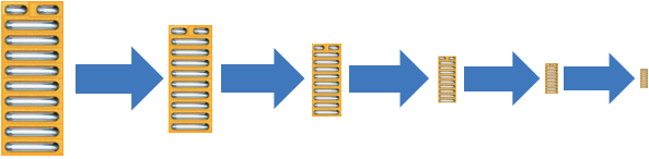 Figure 1: The performance of eGaN FETs is expected to double every two years
resulting in increased performance from a smaller form factor
Beyond just performance and cost improvement, the greatest opportunity for GaN technology to impact the power conversion market comes from its intrinsic ability to integrate multiple devices on the same substrate. In the future, GaN technology, as opposed to common silicon IC technology, will allow designers to implement monolithic power systems on a single chip in a more straightforward and cost-effective way.
Today, the most common building block used in power conversion is the half bridge. This therefore becomes the starting point for the journey towards a power system-on-a-chip.
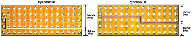
Figure 2: Two eGaN FETs integrated onto one chip forming a monolithic half bridge in a chipscale package. (Bump Side)
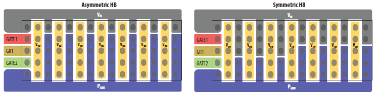
Figure 3: Pinout for the device in figure 2.
In figure 2 are pictures of devices from the first family of commercially available enhancement mode monolithic half-bridge GaN integrated circuits, the EPC2100. Each device has a voltage rating of 30 V. The upper FET (Q1) has a typical RDS(on) of 6 mΩ, and the lower FET (Q2) has a typical RDS(on) of 1.5 mΩ. It comes in a chipscale package for improved switching speed and thermal performance, and has dimensions of 6 mm x 2.3 mm. In figure 3 is the pin-out configuration of the device. Gate 1 is the high side gate pin. GR1 is the high side gate return pin. Gate 2 is the low side gate pin. VSW is the switch node of the half bridge and consists of 35 individual solder pins that are connected in parallel on the PCB. VIN is the input voltage supplied to the drain of the top FET (Q1), and consists of 8 parallel-connected pins. PGND is the power ground connection at the source terminal of the lower FET (Q2) and has 29 parallel-connected solder pins. By integrating the two power FETs into a single monolithic device interconnect inductances and the interstitial space needed on the PCB are eliminated. This increases both efficiency (especially at higher frequencies) and power density while reducing assembly costs.
Table 1 shows the complete family of half-bridge ICs. Note that for three members of the family, the high side FET is approximately one-fourth the size of the low side device. This ratio is to optimize efficient DC-DC conversion in buck converters with a high VIN/VOUT, as shown in figure 4. For applications requiring symmetric die sizes, e.g. brick power supplies, motor drives, and class D audio, there are three members of the family that have equal die sizes for both the high side and low side FETs, as shown in figures 2 and 3.
In each of these first members of the family of half bridge ICs, the high side FET is approximately one-fourth the size of the low side device to optimize efficient DC-DC conversion in buck converters with a high VIN/VOUT ratio such as that shown in figure 4.
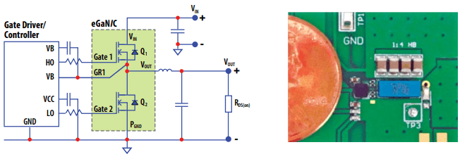
Figure 4: A 12 V
IN, 1.2 V
OUT buck converter. On the left is the circuit schematic and on the right is the actual circuit with the EPC2100 eGaN half bridge.
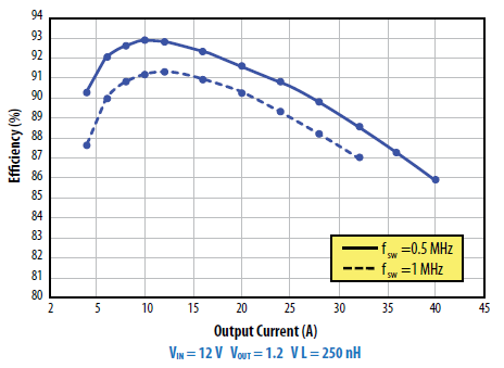
Figure 5: Total buck converter efficiency with the EPC2100 half bridge at 500 kHz and 1 MHz.
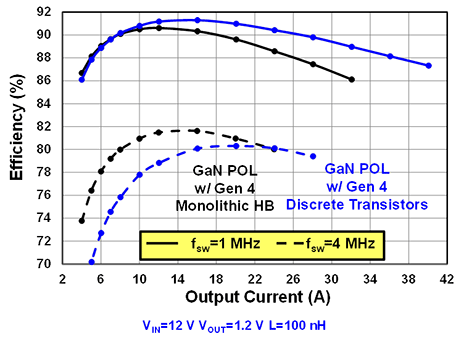
Figure 6: Total buck converter efficiency with the
EPC2100 half bridge compared with discrete eGaN FETs (Q1:
EPC2015; Q2:
EPC2023).
The measured efficiency of this circuit is shown in figure 5. At 500 kHz, peak efficiencies of the complete buck converter approach 93% at 10 A, and at 20 A the efficiency is over 90.5%.
The advantages of increased integration become clearer at higher frequencies. In figure 6 is a comparison between two buck converters operating at 1 MHz and at 4 MHz. The blue lines represent the converter built with discrete eGaN FETs. The black lines represent the buck converter built with the EPC2100 monolithic half bridge. The halfbridge is 33% smaller than the combined die area of the two discrete FETs and, as a consequence, the synchronous rectifier FET (Q2) has about 50% higher on resistance. At low frequency and high current, the buck converter with the monolithic half bridge therefore has lower efficiency. As the frequency is increased to 4 MHz, however, the efficiency of monolithic half bridge overtakes the discrete implementation by about 2% at peak efficiency as shown in figure 6.
The removal of the interstitial space between die, coupled with an optimum power loop layout, results in a significant reduction in the overall power loop inductance to under 200pH – less than half of that reported using discrete EPC2015 devices [2]. This results in voltage transitions in the two-thirds of a nano-second range and an overshoot of only 3.6 V while switching 25A, as shown in figure 7.
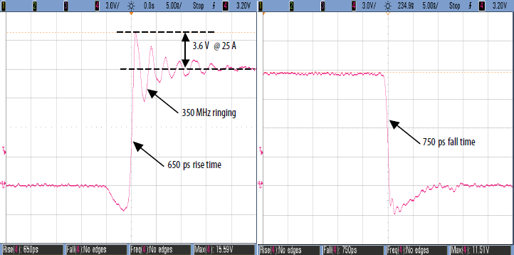
Figure 7: Switch node waveforms for the EPC2100, V
IN = 12 V to V
OUT = 1.2 V, I
OUT = 25 A, 1 MHz showing 650 ps rise time and 750 ps fall time
Now we’ll look at a higher input voltage POL conversion. Figure 8 shows the efficiency of a converter running at 500 kHz with the EPC2101. This 60 V half-bridge eGaN IC can convert much higher bus voltages, such as 28 V and 42 V, directly to 1 V efficiently. Figure 9 is the switch node waveform of this conversion.
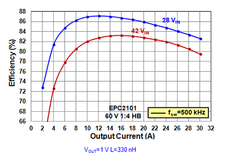
Figure 8: Total buck converter efficiency with EPC2101 half bridge.
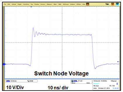
Figure 9: Switch node voltage at V
IN=42 V V
OUT=1 V I
OUT=20 A fsw=500 kHz
Going to even higher input voltage POL conversion. Figure 10 shows the efficiency of a converter running at 500 kHz with the EPC2105. This 80 V half-bridge eGaN IC can convert 48 V directly to 1 V efficiently. At 16 A, peak efficiency of over 80% is achieved for the full buck converter system. This conversion eliminates two stages that are normally required for this voltage conversion in Datacom systems.
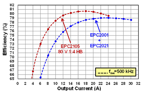
Figure 10: Total buck converter efficiency with EPC2105 half bridge IC compared with discrete eGaN FETs. V
IN = 48 V, V
OUT = 1 V
For applications requiring a more symmetric device ratio, the 60 V EPC2102, the 80 V EPC2103 and the 100 V EPC2104 provide monolithic half-bridge eGaN ICs with two equal sized dies as shown in figure 2. The total system efficiency of a 48 VIN to 12 VOUT POL buck converter is shown in figure 11. For a lower step down ratio with a higher duty cycle, the symmetric half-bridge demonstrates higher efficiency as shown in figure 11. The symmetric half-bridge eGaN IC also demonstrates fast switching speeds with rise and fall times, shown in figure 12, of 2,1 ns and 1.4 ns respectively for 48 V input voltage and 20 A output current.
Discrete eGaN FETs have been in volume production for almost 5 years and have infiltrated many of the traditional applications for silicon MOSFETs. The efficiency gap is growing as this relatively new technology follows a faster learning curve [3]. Now designers have a family of monolithic eGaN half bridge devices that save space, improve efficiency, and lower system costs. As power conversion systems stretch into the multi-megahertz domain, the integration of discrete devices becomes even more important for high system efficiency and power density.
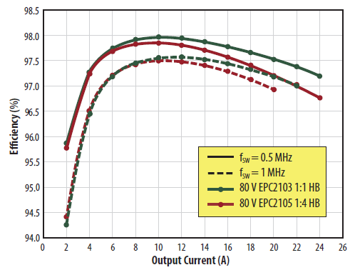
Figure 11: Total buck converter efficiency with EPC2103 and EPC2105 half bridges. V
IN = 48 V, V
OUT = 12 V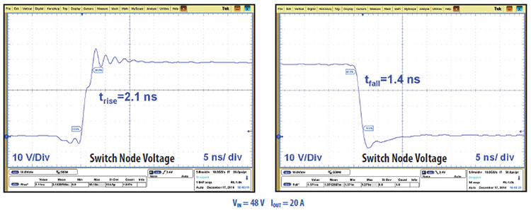
Figure 12: Switch node waveforms for the EPC2103, V
IN = 48 V to V
OUT = 12 V, IOUT = 20 A, showing 2.1 ns rise time and 1.4 ns fall time
References
- A. Lidow, J. Strydom, M. de Rooij, and D. Reusch, “GaN Transistors for Efficient Power Conversion, Second Edition,” J. Wiley, 2015.
- D. Reusch, J. Strydom, “Understanding the Effect of PCB Layout on Circuit Performance in a High Frequency Gallium Nitride Based Point of Load Converter,” APEC 2013, pp.649-655, 16-21 March 2013.
- https://epc-co.com/epc/products/gan-fets-and-ics/Gen4eGaNFETs.aspx
 Download pdf version