Why Is Gallium Nitride Important?
Gallium nitride can can conduct electrons more efficiently and can withstand higher electric fields than silicon. It exceeds the performance capability of silicon in speed, temperature, power handling and is replacing silicon-based devices in a variety of power conversion and RF applications.
The benefits of GaN-based systems include the ability to offer greater efficiency, significantly reduced size and weight, and improved thermal performance. This ability is creating a displacement cycle in traditional silicon markets and enabling new applications, such as remote sensing technology (lidar) and energy storage systems for solar applications.
Can GaN Replace Silicon?
In 1978 the silicon power MOSFETs were launched as a faster alternative to the slower and aging bipolar devices. The early adopters of the power MOSFET were applications where the bipolar just was not fast enough. The signature example for its adoption was the switching power supply for the desktop computer and from there the MOSFET went on to become the power conversion device of choice for the semiconductor industry.
The dynamics of this transition taught us that there are four key factors controlling the adoption rate of a new power conversion technology
- Ability to support new applications
- Ease of use
- Cost-effectiveness
- Reliability.
Now, GaN has assumed the position as the presumptive replacement for the aging power MOSFET, but in order for it to take the mantle as the semiconductor technology of choice, it must meet four requirements that all new technologies must meet to this leadership position.
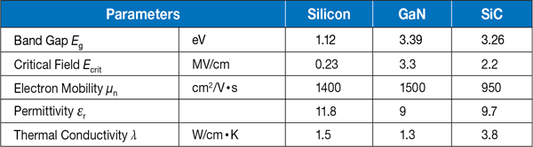
Material properties of GaN, 4H-SiC, and Si:
Why is GaN the Replacement for the Power MOSFET
Let’s take a look at the four key questions that can lead to a new power conversion technology replacing silicon, and see where GaN stands in addressing them.
1. Does GaN Enable New Applications?
The early success of GaN-based power transistors and integrated circuits initially came from the speed advantage of GaN compared with silicon. GaN-on-Si transistors switch about 10 times faster than MOSFETs and 100 times faster than IGBTs. Applications such as RF envelope tracking for 4G/LTE base stations and light detection and ranging (lidar) systems for autonomous cars, robots, drones, and security systems were the first volume applications to take full advantage of GaN’s high-speed switching ability.
Not only were GaN transistors faster than Si MOSFETs and IGBTs, but they were also much smaller – about 5 to 10 times smaller. This opened many applications in robotics and medical electronics as well as satellites and drones.
2. Is GaN Easy to Use?
GaN transistors (specifically enhancement mode, normally ON devices) are very similar in behavior to the aging power MOSFETs, and therefore power systems engineers can use their design experience with minimal additional training. Recent advances in monolithic integration add simplicity beyond that achieved in silicon power devices
To assist design engineers up the learning curve, EPC published the industry’s first GaN transistor textbook (in English and Chinese) – GaN Transistors for Efficient Power Conversion. The third edition was published in 2019 by J. Wiley & Sons. A supplement, GaN Power Devices and Applications, was published in 2021. These textbooks are available through Amazon as well as textbook retailers.
Additionally, more than 100 universities around the world are working with GaN devices to prepare the next generation of highly skilled power system designers to extract the highest performance from this technology.
3. Is GaN a Cost-Effective Alternative to Silicon?
 GaN transistors and integrated circuits from EPC are produced using processes similar to silicon power MOSFETs, have many fewer processing steps, and more devices are produced per manufacturing run because GaN devices are much smaller than their silicon counterparts. In addition, lower voltage (<500 V) GaN transistors do not require the costly packaging needed to protect their silicon predecessors. This packaging advantage alone can cut the cost of manufacture in half and, combined with high manufacturing yields and small device size, has resulted in the cost of a GaN transistor from EPC to be lower in cost than a comparable (but slower, bigger) silicon power MOSFET.
4. Are GaN Devices Reliable?
To date, several manufacturers of GaN transistors have reported excellent results from in-house stress testing. EPC has established a rigorous reliability program which includes testing parts to the point of failure to establish an understanding of the amount of margin between the data sheet limits, and more importantly, an understanding of the intrinsic failure mechanisms. By knowing the intrinsic failure mechanisms, the root cause of failure, and the device’s behavior over time, temperature, electrical or mechanical stress, the safe operating life of a product can be determined over a more general set of operating conditions.
EPC continues to publish results of this testing, and the Phase 15 Reliability report details field reliability data that is unmatched by silicon power devices.
Additional Benefits of GaN
Although the above-mentioned factors are important when it comes to power conversion technologies, they are not the only ones that make GaN stand out. There are more attributes that give GaN a huge advantage over other technologies.
Reduced Size and Weight
GaN devices have a much lower on-resistance per unit area for the same voltage rating compared to both SiC and Si devices. This leads to significantly smaller die and package size.
Theoretical on-resistance for a one square millimeter device vs. blocking voltage capability for Si, SiC, and GaN-based power devices:
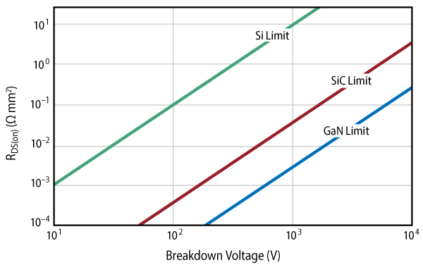
Additionally, from a system perspective the fast-switching speed of GaN allows for higher switching frequencies, enabling a reduction in the size of the passive components, and in some cases elimination of mechanical heatsinking. This results in an overall reduction in the size and weight for the end solution when using GaN FETs and ICs.
Higher Power Density & Higher Efficiency
Due to the significant improvements that GaN offers in switching performance and size reduction, record power density and efficiency can be realized for a multitude of applications.
One example is the 48 V power supplies needed in high-density computing applications for cloud computing, artificial intelligence, machine learning, and gaming applications.
High-efficiency and high-power–density converters enable a reduction in power losses at the system level while allowing smaller form factors. For this application, a GaN-based reference design demonstrated unprecedented levels of power density (> 4 kW/in3) in a 48 V to 12 V power converter with 96.3% peak efficiency and 93.8% when delivering 1 kW into a 12-V load and with module dimensions of 17.5 × 22.8 × 7.7 mm.
Better Thermal Performance
The power consumed in a device during operation is dissipated in the form of heat. It is therefore important to understand the ability of a device to transfer the heat to its surrounding environment. GaN FETs have excellent absolute thermal performance despite the much smaller FET area compared to equivalent RDS(on) MOSFETs. In fact, for chip-scale GaN transistors, the thermal resistance to case (RθJC) is lower than silicon devices, and thus the junction-to-case path provides good thermal conductance.
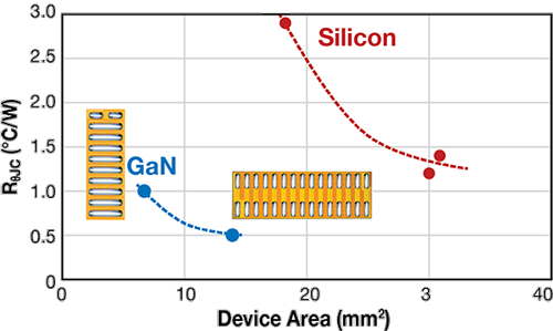
Additionally, simple, and practical heat sink mounting methods exist to extract even more heat and extend the output current capability of GaN-based designs.
Conclusion
The four requisite attributes for GaN to displace the silicon MOSFET have been achieved. But this is just the beginning for GaN. Even the latest devices on the market are about 300 times larger than they would be if they could be made at the theoretical limits for GaN.
The most significant opportunity for GaN to impact the performance of power conversion systems and prove its many benefits comes from the intrinsic ability to integrate both power-level and signal-level devices on the same substrate. EPC has been producing GaN ICs since 2014 with the goal to drive toward complete systems on a single GaN-on-Si chip where the user supplies a logic level input and out comes high-performance power conversion. Smaller, faster, lower cost, and more integrated…so in summation, this is our answer to the question “Why GaN?”.
How Can GaN Be Used?

Aerospace and Defense

Consumer Electronics

MedTech

Communications