Alex Lidow, PhD, David Reusch, PhD, Johan Strydom, PhD
Fourth generation of GaN-on-silicon enhancement mode transistors (eGaN FETs) sets new performance records. This family of products range from 30 V to 200 V and significantly widen the performance gap between the aging power MOSFET and gallium nitride-based transistors.
Gen 4 Device Family Overview
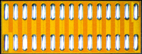 Figure 1: Mounting side of 30 V EPC2023 eGaN FET
In this application note we present the key improvements embodied in the latest generation of eGaN FETs. That will be followed by two application examples, a 12 V - 1.2 V converter and a 48 V - 12 V converter; both with unprecedented performance. Table 1 shows the basic device parameters for the Gen 4 products. Representative Gen 2 products are also shown for comparison in the shaded rows at the bottom of the table. Lower on-resistance (RDS(on)), lower capacitance, higher current, and superior thermal performance characterize this family of eGaN FETs.
Die Layout:
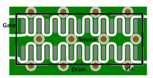 Figure 2: Plot of a possible PCB layout for the die in figure 1
Since their initial launch in 2010, eGaN FETs have had extremely low on-resistance in an extremely small footprint compared with any previously available semiconductor [1]. The Gen 4 products continue this tradition with the chipscale LGA footprint shown in figure 1. Interleaved drain and source bars help reduce the power loop inductance while internal design virtually eliminates common source inductance. To improve the thermal and electrical, the largest devices of the Gen 4 family have a gap between the top row of solder bars and the bottom row. This gap in the middle of the die enables large copper traces along with cooling vias in the PCB for enhanced thermal performance. A sample layout of the 2 ounce copper top layer is shown in figure 2. Using 12 mil vias with 22 mil annular rings on 1.6mm centers help remove the heat from the area surrounding the device as well as from the center of the transistor. This configuration also supports the use of our optimal layout power loop structure [2] while using 4 ounces or more of copper on the inner layers.
Table 1
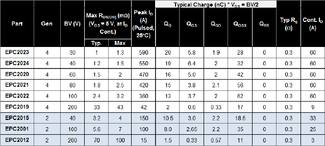
* Preliminary Data - subject to change without notice
On-Resistance:
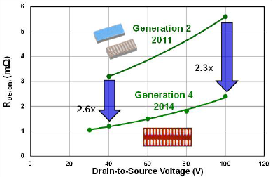 Figure 3: On-resistance comparison of previous and latest generation eGaN FETs
Previously, to increase the output current in eGaN FET-based DC-DC converters, paralleling of multiple devices was required [3]. While paralleling high performance eGaN devices could provide higher output power, the increased part count adds cost and complexity while reducing the power density of the system. The new family of eGaN FETs demonstrates a significant reduction in on-resistance, (RDS(on)), enabling high current, high power density eGaN FET-based DC-DC converter applications. In figure 3 the latest generation of eGaN FETs with voltages range from 30 V to 100 V and on-resistances range from 1.0 to 2.4 mΩ are shown. A 200 V FET, EPC2019, is also part of the Gen 4 family and has a typical on-resistance of 33 mΩ in an ultra-small footprint.
Hard Switching Figure of Merit (FOMHS) [4]:
In a traditional hard-switching transition, the switching losses are impacted primarily by two device parameters, QGD, the gate-to-drain charge (also known as the Miller charge), which controls the voltage rising and falling transition time; and QGS2, which is the portion of the gate-to-source charge from the device threshold voltage to the gate plateau voltage, which controls the current rising and falling transition time. The hard switching figure of merit (FOMHS) given below can be used to compare the in-circuit performance capability of a given device technology in different hard-switched applications.
FOMHS = (QGD + QGS2) ∙ RDS(on)
The latest generation of eGaN FETs demonstrates an almost 2x reduction in FOMHS over the previous generation as shown in figure 4(a). The newest family of eGaN FETs reduces FOM by 3.5x, 6.1x, and 8.5x respectively for 40 V, 100 V, and 200 V devices when compared to the best state-of-art Si power MOSFETs. With lower FOMHS, improved device packaging, and low parasitic PCB layout, the high frequency performance of high density eGaN FET-based converters is significantly improved compared to Si MOSFETs.
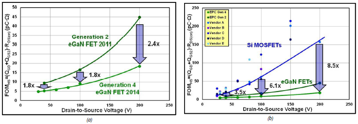 Figure 4: Hard switching FOMHS comparison of (a) previous and latest generation eGaN FETs (b) eGaN FETs and state-of-the-art Si power devices
Soft Switching Figure of Merit (FOMSS) [5]:
In resonant and soft-switching applications the switching-related losses are minimized by using techniques such as zero voltage switching (ZVS) and zero current switching (ZCS). With the reduction of switching losses, the FOMHS used for hard switching applications to compare device technologies is no longer valid for soft-switching applications.
In most soft-switching applications the device output charge, QOSS, has a large impact on performance as it directly impacts the energy required to achieve ZVS. A reduction in energy required to achieve ZVS can result in reduced dead times and ZVS currents, providing both a larger power delivery period and lower RMS currents in high frequency soft-switching and resonant converters. QOSS is also the main loss component in ZCS switching. The other major contributor to loss is the gate charge, QG, which is a major switching related loss in high frequency soft-switching applications. A soft switching figure of merit can therefore be derived as:
FOMSS = (QG + QOSS) ∙ RDS(on)
The latest generation of eGaN FETs demonstrates 1.3X reduction in FOMSS over the previous generation as shown in figure 5(a). The newest family of eGaN FETs reduces FOM by 1.7x, 2.3x, and 3.5x respectively for 40 V, 100 V, and 200 V devices when compared to the best state-of-art Si power MOSFETs. With lower FOMSS, improved device packaging, and low parasitic PCB layout, the high frequency performance of high density eGaN FET-based converters is significantly improved compared to Si MOSFETs is soft switching as well as hard switching applications.
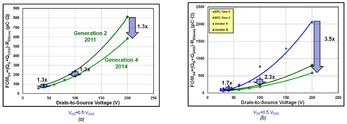 Figure 5: Soft switching FOMSS comparison of (a) previous and latest generation eGaN FETs (b) eGaN FETs and state-of-the-art Si power devices
Miller Ratio [6]:
eGaN FETs are exposed to significantly higher voltage and current slew rates that can impact the performance of the transistor. These conditions need to be understood well in order to fully utilize the technology. A high, positive-voltage slew rate (dv/dt) on the drain of an off-state device can occur in both hard- and soft-switching applications, and is characterized by a quick charging of the device’s capacitances. During this dv/dt event, the drain-source capacitance (CDS) is charged. Concurrently, the gate-drain (CGD) and gate-source (CGS) capacitors in series also are charged. The concern is that, unless addressed, the charging current through the CGD capacitor will flow through and charge CGS beyond Vth and turn the device on. This event, sometimes called Miller turn-on, can be very dissipative.
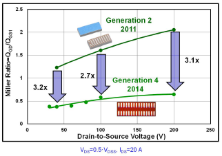 Figure 6: The Miller ratio of Generation 4 devices is superior to Generation 2 and reduces sensitivity to dv/dt-induced false turn-on
To determine the dv/dt susceptibility of a power device, a Miller charge ratio (QGD/QGS1), as function of drain-to-source voltage, can be evaluated. A Miller ratio of less than one will guarantee dv/dt immunity [6]. In figure 6 is shown the large reduction in Miller ratio in Gen 4 FETs, with all of the new-generation product falling under a value of 1 at half their rated voltage.
Experimental Results:
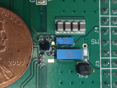 Figure 7: Photo of 12 V – 1.2 V buck converter using Generation 4 eGaN FETs. This buck converter achieves over 91.5% efficiency at 1 MHz
To highlight the improved performance of Gen 4 eGaN FETs, two buck converters were built using a combination of the Generation 4 eGaN FETs as the synchronous rectifier and Generation 2 eGaN FETs as the control device (see figure 7). The first of these converters combined the 30 V, EPC2023 (Gen 4) with the 40 V EPC2015 (Gen 2) in a 12 V – 1.2 V DC-DC point of load (POL) converter. A 48 V – 12 V POL was constructed with an 80 V EPC2021 combined with a 100 V EPC2001.
Shown in figure 8(a) are the experimental results of the 12 V to 1.2 V, 40 A POL converter operating at switching frequency of 1 MHz achieving efficiencies above 91.5% and demonstrating the superior in-circuit performance of the latest generation of eGaN power devices compared to the previous generation of eGaN FETs (shown in green), and state-of-the-art Si MOSFET modules (shown in red). Shown in figure 8(b) are the experimental results of a 48 V to 12 V, 30 A non-isolated DC-DC intermediate bus converter operating at a switching frequency of 300 kHz achieving efficiencies above 98%, again significantly outperforming the previous eGaN FETs, shown in green, and state of the art Si power MOSFETs, shown in red.
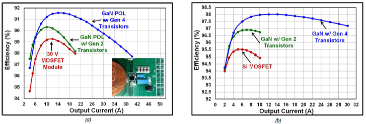 Figure 8: Efficiency comparison between eGaN FET and Si based (a) 12 VIN, 1.2 VOUT, 1 MHz POL converters and (b) 48 VIN, 12 VOUT, 300 kHz non-isolated intermediate bus converters
The improved performance also enables higher frequency operation without sacrificing an enormous amount of efficiency. Figure 9 shows the 12 V to 1.2 V buck converter efficiency at various PWM frequencies. At 0.5 MHz the converter achieves almost 94% peak efficiency. This peak efficiency drops to 87.5% at 2 MHz.
The 48 V to 12 V converter also shows great resilience to higher frequencies with an efficiency of 96% at 1 MHz (see figure 10).
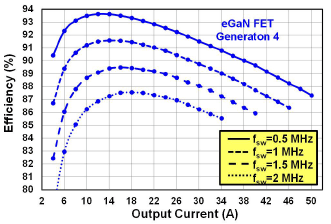 Figure 9: 12 VIN, 1.2 VOUT Gen 4 efficiency at various frequencies
 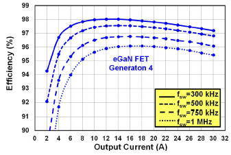 Figure 10: 48 VIN, 12 VOUT Gen 4 efficiency at various frequencies
Summary
In this application note the new 4th Generation eGaN FETs have been introduced. eGaN FETs continues to raise the bar for power conversion performance. In onresistance and in hard-switching applications the Gen 4 family of eGaN FETs doubles the performance of prior generations. The result is a quantum step in efficiency in DC-DC converters.
References
- A. Lidow, J. Strydom, M. de Rooij, and Y. Ma, “GaN Transistors for Efficient Power Conversion, First Edition,” Power Conversion Publications, 2012.
- D. Reusch, J. Strydom, “Understanding the Effect of PCB Layout on Circuit Performance in a High Frequency Gallium Nitride Based Point of Load Converter,” APEC 2013, pp.649-655, 16-21 March 2013.
- D. Reusch and J. Strydom, “Improving Performance of High Speed GaN Transistors Operating in Parallel for High Current Applications,” PCIM Europe 2014, pp. 302-309, 2014.
- D. Reusch, “Improving System Performance with eGaN® FETs in DC-DC Applications,” 46th International Symposium on Microelectronics, iMAPS 2 October 2013.
- D. Reusch and J. Strydom, “Evaluation of Gallium Nitride Transistors in High Frequency Resonant and Soft-Switching DC-DC Converters,” Applied Power Electronics Conference and Exposition, pp. 464 –470, 2014.
- T. Wu, “Cdv/dt Induced Turn-On In Synchronous Buck Regulators”, white paper, International Rectifier Corporation.
 Download pdf version