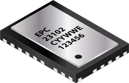
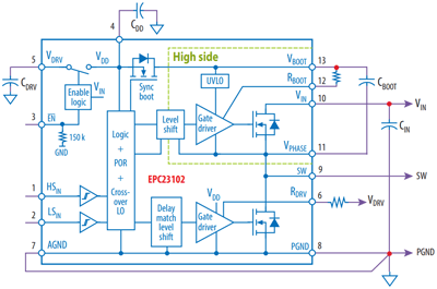
Integrated high side and low side eGaN® FETs with internal gate driver and level shifter
Power Stage Load Current (1 MHz), 35 A
Maximum Input Voltage, 100 V

Package Size: 3.5 mm x 5 mm
Features
- 5 V external bias supply
- Independent high side and low side control inputs
- 3.3 V or 5 V CMOS input logic levels
- Logic lockout commands both FETs off when inputs are both high at same time
- External resistors to tune SW switching times and over-voltage spikes above rail and below ground
- Robust level shifter operating for hard and soft switching conditions
- False trigger immunity from fast switching transients
- Synchronous charging for high side bootstrap supply
- Disable input engages low quiescent current mode from VDRV supply
- Power on reset for low side VDD supply
- Undervoltage lockout for high side VBOOT supply
- Active gate pull-down for HS FET and LS FET with loss of VDRV supply
- Thermally enhanced QFN package with exposed top for low thermal resistance from junction to top-side heatsink
Applications
- Buck, Boost, Buck-Boost Converters
- Half-Bridge, Full Bridge LLC Converters
- Motor Drive Inverter
- Class D Audio Amplifier

Status: Engineering
Engineering devices, designated with an ENG* suffix at point of purchase, are on engineering status and should not be used for reliability stress testing or other qualification testing without contacting your local field application engineer for the latest status.