How Picotest Uses eGaN FETs to Design Groundbreaking High-Speed Transient Load Current Steppers - Revolutionizing Power System Testing for Data Center, AI, EV, ASIC, and Server Applications
GaN Talk – Renee Yawger
Feb 08, 2024
Picotest, renowned for its custom test equipment in power integrity and power systems testing, has just launched a groundbreaking series of high-speed transient load current steppers using a previously unseen level of gallium nitride (GaN) integration. This latest innovation is poised to redefine industry standards, particularly in demanding low-voltage, high-current applications, such as data centers, AI, graphics, EV, ASIC test, and servers. These load steppers bring forth a range of capabilities that address critical challenges in power integrity testing.
Powering the Future
The Voltage Regulation Module (VRM) and power distribution network (PDN) validation, essential for start-up, dynamic transient performance, stability, and noise assessments, necessitate swift load current transitions, high peak and average power, and adaptable form factors. Picotest's revolutionary load steppers utilize GaN technology, innovative power delivery formats, and advanced cooling mechanisms to meet the stringent requirements of these power systems.
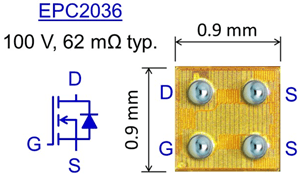
Featured GaN FET
The featured GaN FET, shown in the image below, is the 100 V rated EPC2036 available in a 2 x 2 bump BGA CSP and has a typical RDSon of 62 mΩ.
Problems Addressed and Breakthrough Solutions
- Critical Power Integrity Design
Good power integrity design is paramount for system performance and product reliability. The load steppers address the need for verifying and validating PDNs through impedance and load step transient performance testing.
- Avoiding Costly Damages
These load steppers eliminate the risk of dynamic load transients damaging expensive digital loads like CPUs, ASICs, FPGAs, and other custom ICs. They also allow vetting of the power systems that are critical to IC test fixtures.
- Overcoming Limitations of Electronic Loads
Traditional electronic loads are often too slow, present excessive capacitance, and lack the necessary edge rates to address bandwidths needed for PDN performance testing. The load steppers overcome these limitations with their high bandwidth, elevated power/current capabilities, and innovative form factors.
- Technological Breakthroughs
To achieve these breakthroughs, Picotest pushed the boundaries of GaN power density, developed custom resistors, employed advanced cooling techniques, and integrated high-speed digital control. The reduction to near-zero inductance in the interconnect between the steppers and the PCB, where the load step is applied, was key to achieving the edge rates required for testing high bandwidths.
Why GaN?
Extreme Speed
The higher electron mobility of GaN compared to silicon allows for significantly faster switching speeds. GaN has a wider bandgap than silicon, which also contributes to faster switching speeds, as it allows for quicker transitions between the on and off states. Additionally, GaN FETs exhibit lower parasitic capacitance compared to silicon MOSFETs. The reduced capacitance enables faster charge and discharge times during switching, resulting in quicker transitions.
- In this application of high-speed transient load steppers for VRM and PDN validation, the extremely fast switching capability of GaN transistors contributes to the ability to generate precise and fast transient load conditions, allowing engineers to assess the performance and stability of power delivery systems under dynamic operating conditions.
High Current Density
GaN FETs exhibit lower on-resistance per area compared to silicon MOSFETs allowing more efficient current conduction, leading to less power dissipation and the capability to carry higher currents. The higher electron mobility of GaN allows for faster charge transport, which also results in the ability to handle higher current densities.
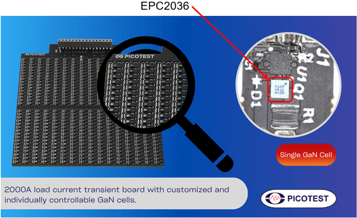
- In this application, each EPC2036 GaN FET can carry 5 A in a tiny 0.9 mm x 0.9 mm footprint. This allows for an unprecedented level of GaN integration; the 2000 A load board consists of 512 load cells using ultra-fast GaN switches to achieve up to 2047 Amps in 100 mm x 100 mm footprint. Each load cell is approximately 2.5 mm x 5.5 mm, smaller than a typical grain of rice, and capable of up to 5 A per cell. This allows scaling from inside a probe tip.
Groundbreaking Design with GaN FETs for Power System Testing
Picotest's high-speed transient load current steppers mark a transformative moment in the field of power systems testing. By overcoming existing limitations and introducing unprecedented capabilities, including a previously unseen level of GaN integration, these innovations are set to redefine industry standards, particularly in demanding low-voltage, high-current applications, such as data centers, AI, graphics, EV, ASICs, and servers.