Sign up today to get the latest news and updates from EPC on new product announcements, applications work, and much more. Sign up for EPC email updates.

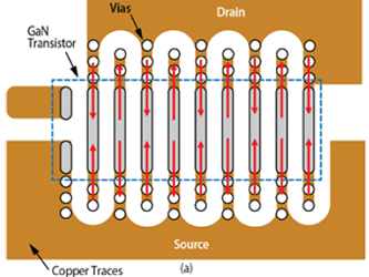
Gallium nitride (GaN) transistors have been in mass production for over 10 years. In their first few years of availability, the fast switching speed of the new devices – up to 10 times faster than the venerable Si MOSFET – was the main reason for designers to use GaN FETs. As the pricing of GaN devices normalized with the MOSFET, coupled with the expansion of a broad range of devices with different voltage ratings and power handling capabilities, much wider acceptance was realized in mainstream applications such as DC-DC converters for computers, motor drives for robots, and e-mobility bikes and scooters. The experience gained from the early adopters has led the way for later entrants into the GaN world get into production faster. This article is the first in a series of articles discussing three topics that can help power systems designers achieve the most out of their GaN-based designs at the lowest cost. The three topics are: (1) layout considerations; (2) thermal design for maximum power handling; and, (3) EMI reduction techniques for lowest cost.
Bodo’s Power Systems
January, 2021
Read article