eGaN Technology Reliability and Physics of Failure - Thermo-mechanical board level reliability of eGaN devices
GaN Talk – Chris Jakubiec
Jan 13, 2017
eGaN® Technology Physics of Failure
The first three installments in this series covered field reliability experience and stress test qualification of Efficient Power Conversion (EPC) Corporation’s enhancement-mode gallium nitride (eGaN®) field effect transistors (FETs) and integrated circuits (ICs). Excellent field reliability that was documented is the result of applying stress tests covering the intended operating conditions the devices will experience within applications. Of equal importance is understanding the underlying physics of how eGaN devices will fail when stressed beyond intended operating conditions (e.g. datasheet parameters and safe operating area). This installment will take a deeper dive into the physics of failure centered around thermo-mechanical reliability of eGaN wafer level chip-scale packages (WLCSP).
EPC FETs and ICs are offered in various wafer level chip-scale packages. The advantages of delivering power FET devices in WLCSP are faster switching speeds, lower on-resistance, lower thermal resistance, improved reliability, and lower cost. Traditional plastic molded power device packages include leads and pads to provide connections to the printed circuit board (PCB), whereas solder bumps and solder land grid arrays are used in EPC chip-scale packages. This evolution to a significantly higher performing and lower cost power package is accompanied by a need to understand the thermo-mechanical capability of solder mounted eGaN devices, which in turn can provide high board-level reliability in the field. Figure 1 shows examples of EPC eGaN devices in solder land grid array (a) and solder bump (b) chip-scale packages.

Figure 1. (a) EPC2007C chip-scale package solder land grid array.
(b) EPC2032 chip-scale package solder bump.
Thermo-Mechanical Reliability
EPC chip-scale devices are without plastic encapsulation, bond wires, and die attach materials included in traditional power packages. With the elimination of these package interfaces that can fail under thermal stresses, the main area of focus in the chip-scale package is the die to PCB solder joint reliability.
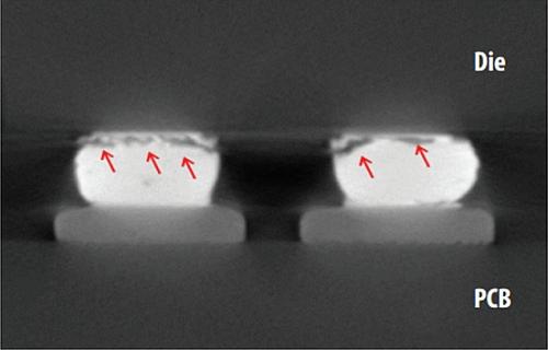
Solder joint stress comes from temperature fluctuations within the die, solder joint, and PCB. More specifically, the global coefficient of thermal expansion (CTE) mismatch between the three attaching materials accounts for the majority of solder joint stress. During temperature excursions above and below ambient, the die (CTE ~ 3 ppm/° C) and typical FR4/FR5 PCB (CTE ~ 10-16 ppm/° C) substrates will expand and contract at different rates. As the die and PCB move at different rates under the influence of temperature, a shear strain will develop in the solder joint connecting the two. Generally, after many temperature cycles the repeated effect of the shear strain on the solder joint will result in fatigue and ultimately fractures (see Figure 2 for example). In addition to degraded or complete loss of signals, the fractured solder joints can result in higher die temperatures due to the loss of the conductive thermal dissipation path to the PCB traces. A local CTE effect within the solder joint also exists, however it is not the dominant fatigue mechanism and will not be examined here.

Figure 2. Cracked solder joints resulting from intermittent operating life stress testing.
Thermo-Mechanical Stress Testing & Modeling
As previously described in the 3rd installment of this blog, there are two main industry accepted stress test methods to evaluate thermo-mechanical reliability. Temperature cycling (TC) is done in an unbiased condition by cycling the ambient temperature between two levels (typical conditions for qualification of EPC devices -40° C to +125° C). Intermittent Operating Life (IOL) stress test uses increased cyclic power to heat the device junction temperature (TJ) to a predefined level, and subsequently lowers the power to return the junction temperature to the starting condition (a typical cycle might be Δ TJ = 100° C). EPC is using both TC and IOL stress tests to evaluate eGaN device thermo-mechanical capability. Cumulative stress tests results including TC and IOL, were also included in the previous installment.
As might be expected larger differences in CTE of the die and PCB as well as peak temperature differences, result in more strain on the solder joints per thermal stress cycle. Other first order effects that contribute to the magnitude of solder joint strain, are the distance of the solder joint from the neutral point of the die, and the solder joint standoff height. The following equation can be used to estimate the thermo-mechanical shear strain at a solder joint, and demonstrates the relationship of primary contributing factors [from 1]:
ε = Δα × ΔT(DNP/t)
where ε is the shear strain in the solder joint, Δα is the CTE difference between die and PCB, ΔT is the cyclic temperature change, DNP is the distance of solder joint from die neutral point, and t is the solder joint standoff height.
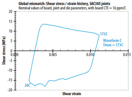
EPC has ongoing experiments to investigate accelerated thermo-mechanical stress test conditions, with the goal of developing predictive lifetime models based on number of thermal cycles to failure. The approach is to create lifetime models based on calculated strain energy on the solder joints during thermal cycling, while testing the device solder joints to failure using several different Δ TJ profiles. The initial preliminary lifetime model was done using the IOL stress test with four different cyclic temperature profiles (Δ TJ = 100° C, Δ TJ = 125° C, Δ TJ = 138° C, Δ TJ = 150° C) on a EPC80xx (2.1 mm x 0.9 mm) land grid array device. A corresponding cyclic stress-strain energy density was calculated for each temperature profile using the methods described in “Acceleration Factors and Thermal Cycling Test Efficiency for Lead-Free-SN-AG-CU Assemblies” [2]. Figure 3 shows an example of the modeled stress-strain energy density per cycle, in a solder joint subjected to a Δ TJ = 150° C IOL temperature profile. The X and Y axes show the contributions of shear strain and stress on the solder joints as the device is cycled through the temperature range. The area inside the loop represents the total plastic (creep) strain energy density per temperature cycle.

Figure 3. Calculated solder joint strain energy density during IOL cycle Δ TJ = 150° C (EPC80xx: 2.1 mm x 0.9 mm)
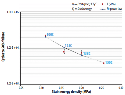
The IOL stress test for each of the four temperature conditions was done until 50% (also known as T50) of the test population failed. Figure 4 shows the calculated strain energy density versus number of cycles to T50 failures. A power law curve (exponent -2) was found to give the best fit to the data, with the following general equation used to predict number of cycle to failure (Nf):
Nf = (260 cycles) x ES-2
Where ES is the strain energy.

Figure 4. IOL thermal model: number of cycles to failure (T50) vs. solder joint strain energy density (error bars represent 67% confidence)
EPC has established a preliminary model for predicting solder joint lifetime based on applied thermo-mechanical stress, that can be used to estimate number of thermal cycles to failure for a particular operating condition. Additional testing of various EPC devices is ongoing to further validate this thermal lifetime model, as well as temperature cycle stress tests to corroborate the results.
Summary
Thermo-mechanical board level reliability of eGaN devices must be understood to properly function in a wide range of end-user field applications over expected lifetimes. EPC eGaN FETs and ICs in wafer level chip-scale packages are a paradigm shift from traditional plastic FET power packages. As such, EPC is performing extensive thermo-mechanical stress testing and modelling to understand the physics of failure, and demonstrate lifetime capability. The next installment will continue to look into physics of failure of eGaN devices, specifically examining gate reliability.
References
[1] Bongtae Han and Yifan Guo, “Determination of an Effective Coefficient of Thermal Expansion of Electronic Packaging Components: A Whole-Field Approach”, IEEE Transactions on Components, Packaging, and Manufacturing Technology – Part A, Vol. 19, NO. 2, June 1996.
[2] Jean-Paul Clech, “Acceleration Factors and Thermal Cycling Test Efficiency for Lead-Free SN-AG-CU Assemblies”, EPSI Inc., 2005.
[3] C. Jakubiec, R. Strittmatter, C. Zhou, “EPC eGaN FETs Reliability Testing: Phase 8,” 2016,