More Data, More Apps, More Mobile…
GaN Talk – Renee Yawger
Oct 18, 2017
I don’t know about you, but in my house the number of mobile devices seems to multiply overnight, along with the ways they are used. On any given night, you may find me on a GoToMeeting conference on my laptop, my husband on a video Skype chat from his phone with his dad in Florida, my oldest son turning in an assignment on Google Classroom from his laptop, my younger son streaming videos on his tablet, and my second grader recording and posting a music.ly on her phablet. And when we travel, these devices come with us so they need to be small and lightweight enough to come along for ride!
This all translates into ever-increasing power demands for computing and telecom systems and the conflicting desire for small, lightweight form factors, and extended battery life. To meet these demands, point-of-load (POL) DC-DC converters (the power engines) need to be designed to be small sized and as efficient as possible. These demands translate to ever faster switching frequencies of the transistors used in the power conversion running these devices. Notebook PCs, tablets, and phablets are especially sensitive to this need as our dependency on these devices and the demands we make on them continues to grow.
The power conversion circuits in these systems occupy nearly half of the space and literally defines the maximum height of the motherboard. Since passive components dominate the size of the power electronics, the most straightforward way to achieve a size reduction is to increase switching frequency, enabling a reduction in the size of the output capacitance and inductance. The ability of gallium nitride (GaN) based power devices to operate efficiently at high frequency will drive significant size reductions of next generation mobile computing.

Figure 1: Tablet, notebook PC, phablet
Increase Speed Without Sacrificing Converter Efficiency...Through Integration
Increasing frequency is a proven method to reduce size. Equally important for mobile systems is to achieve a high efficiency solution, a key to saving battery life. Converter efficiency can be significantly improved with single-chip integration of eGaN FETs.
A key speed bump on the road to high frequency and efficiency is parasitic inductance. Parasitic inductance not only induces unwanted voltage stresses but have been demonstrated to reduce switching speeds [1]. By integrating two eGaN power transistors (FETs) into a single device, interconnect inductances and the interstitial spacing needed on the PCB are greatly reduced or even eliminated.
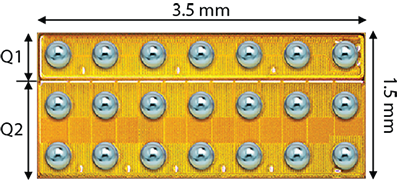
A second advantage of integration is the ability to optimize die size of both the control FET and the synchronous rectifier. Integration allows for the reduction in size of the control FET (Q1) to reduce the switching related losses and a larger synchronous rectifier (Q2) to reduce conduction losses. The EPC2111 (Figure 2) is a monolithic eGaN half-bridge IC designed for high step-down point-of-load (POL) converters where the control FET (Q1) is approximately one fourth the size of the synchronous rectifier (Q2).
A third advantage of integration is improved thermal performance. Monolithic integration allows highly efficient heat transfer from the smaller sized control device (Q1) to the larger rectifier device (Q2), giving more balanced heat distribution in the system as well as a more efficient path to distribute heat from the devices to the PCB [1].

Figure 2: EPC2111, 30 V eGaN half bridge
Monolithic integration paves the way for higher switching frequency at high efficiency in point-of-load converters. The small footprint further increases power density to keep pace with demanding application requirements.
High Speed Gate Drivers Take Advantage of GaN Capabilities
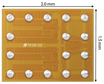
New gate drivers are arriving in the marketplace that take advantage of the high frequency switching capabilities of GaN. One such device, the PE29102 from Peregrine Semiconductor, is an integrated high-speed driver with outputs capable of providing switching transition speeds in the sub-nanosecond range for hard switching applications up to 33 MHz. The PE29102 is optimized for both matched dead time and propagation delay to improve system bandwidth. Available in a compact, flip-chip package, further reduces the parasitic inductance of the system design and ultimately saves board space.

Figure 3: PE29102, High-speed GaN FET driver
10 MHz Point-of-Load Conversion
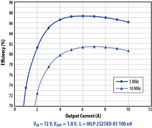
Today’s point-of-load systems typically operate at 1 MHz and below. By pairing the 30 V EPC2111 eGaN half bridge with the Peregrine PE29102, a complete overall point-of-load system converting 12 V to 1.8 V achieves efficiency levels of 86% at 10 A when switching at 5 MHz and over 80% when switching at 10 MHz (Figure 4). Increasing the switching frequency of the power transistors from the typical 1 MHz of today’s designs to 10 Mhz, will result in an estimated 56% reduction in board area and an estimated 65% reduction in height

Figure 4: Typical efficiency for V
IN = 12 V to 1.8 V
OUT POL converter
More Data, More Apps, More Mobile
We want our mobile devices to perform an ever-growing array of power-hungry tasks yet remain small and lightweight. Reducing the size and decreasing the power consumption of the core power electronics is critical to keep pace with these demands. Increasing the switching frequency of power transistors is a known path to size reduction. GaN based power devices, available today, help eliminate the speed bumps to higher converter frequencies and will drive the next generation of mobile computing. I can already imagine the hours of SnapChat and streaming Minecraft videos my family will enjoy ….