How to Get More Power Out of a High-Density eGaN-Based Converter with a Heatsink
GaN Talk – Rick Pierson
Dec 14, 2018
Motivation
eGaN® FETs and ICs enable very high-density power converter design, owing to their compact size, ultra-fast switching, and low on-resistance. The limiting factor for output power in most high-density converters is junction temperature, which prompts the need for more effective thermal design. The chip-scale packaging of eGaN also offers six-sided cooling, with effective heat extraction from the bottom, top, and sides of the die. This application note presents a high-performance thermal solution to extend the output current capability of eGaN-based converters.
Thermal solution for six-sided cooling
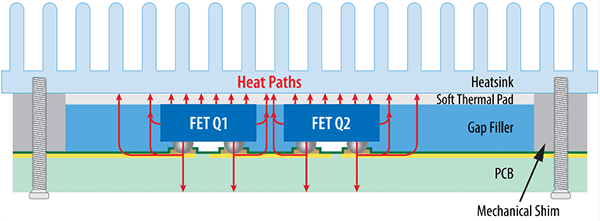
The thermal solution depicted in Figure 1 enables excellent heat extraction from chip-scale eGaN FETs, as previously demonstrated in [1] and [2]. A heatsink is mechanically attached to the board using screws and a plastic shim, enclosing an area filled with electrically isolating thermal interface material (TIM). The TIM conducts heat directly from the top and sides of the FET to the heatsink. This provides the most effective thermal path, owing to the very low Rθ,jc of eGaN FETs and ICs. Simultaneously, the FETs conduct heat to the PCB copper through the solder bumps, which is also conducted to the heatsink through the TIM. Additional heat is dissipated through convection on the bottom side of the PCB.
 Figure 1: Simplified cross-section of the thermal solution for chip-scale eGaN FETs, highlighting heat flux paths and mechanical assembly
The height of the shims and thickness of the thermal pad are carefully selected to prevent excessive mechanical stress on the eGaN FETs. The thickness of TIM between the heatsink and FETs should be kept to a minimum to provide the lowest thermal resistance. However, the maximum heights of all components within the shim-enclosed must be considered when selecting the shim thickness, including the FETs, capacitors, and gate driver. Height tolerance and die tilt may both be important factors in this analysis.
Design Flexibility: The TIM can be composed of a soft thermal pad (e.g., t-Global TG-X), a liquid gap filler (e.g., Bergquist GF4000), or a combination of both. The liquid gap filler alone can be used as the TIM, thereby applying near zero compression force to the FETs, however a thermal pad typically has superior thermal conductivity. Similarly, the thermal pad can be used without the liquid gap filler, but this option does not offer heat conduction from the sides of the FET or the PCB to the heatsink. The thermal solution in Figure 1 shows how both TIMs can be implemented to achieve the most effective thermal path while also minimizing mechanical stress on the FETs.
Design example: high-density 48 V to 12 V conversion using the EPC2045 eGaN FET
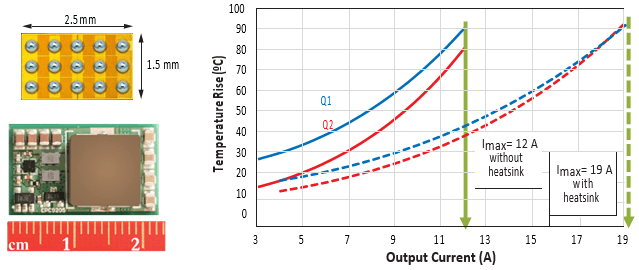
The proposed thermal solution was experimentally demonstrated using the design example shown in Figure 2, which is similar to the EPC9205 GaN power module. This high-density buck converter uses the 100 V EPC2045 eGaN FET to achieve a peak efficiency of 96.4%, when converting 48 V to 12 V at a switching frequency of 700 kHz, and can output up to 12 A with less than 100°C rise in junction temperature.
 Figure 2: Mechanical assembly steps to implement the thermal design using a plastic shim, liquid gap filler, thermal interface pad, and a heatsink
Figure 2 presents a step-by-step guide used to assemble this thermal design:
- A Nylon shim is used to enclose the power stage and provide mechanical support for the heatsink. The shim height in this example is 1.02 mm, which is 0.13 mm taller than the seated height of the EPC2045 (Figure 2a).
- The power stage are enclosed by the shim is then covered with liquid gap filler (Figure 2b).
- A soft thermal interface pad is attached to the bottom of the heatsink. In this example, the pad has 0.5 mm thickness before compression (Figure 2c).
- Finally, the heatsink and pad are placed on top of the liquid gap filler, and clamped down securely to the Nylon shim using two screws. Excess gap filler is cleaned off, and the remainder is allowed to cure to a solid form (Figure 2d).
Thermal performance
The thermal equivalent circuit and current capability are evaluated using the methodology presented in [2], demonstrating a 50% reduction in the junction-to-ambient thermal resistance (Rθ,ja) of each FET when the thermal solution was implemented. However, thermal coupling between the two FETs and output filter inductor must also be considered in this high-density design. Figure 3 shows the current- handling capability of the converter before and after the thermal solution is implemented. The current-handling capability is increased by 60% with the heatsink.
 Figure 3: EPC2045 buck converter junction temperature rise vs. output current for 48 VIN to 12 VOUT when operating at 700 kHz with 800 LFM air flow
Introducing EPC2206 for automotive applications
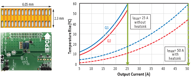
The EPC2206 AEC-qualified 80 V eGaN FET is used here as a design example, to demonstrate that this thermal solution can also be applied to higher-power board designs, with a larger die and power stage. In this example, the maximum allowable temperature rise is 60°C, based on the more extreme environmental conditions of an automotive application. The EPC9034 development board was used for evaluation, with the output inductor located off-board. Adding a heatsink decreases each FET’s Rθ,ja by 60%, effectively doubling the output current capability from 25 A to 50 A as shown in Figure 4. Only the soft thermal pad is used in this example, such that further improvement is possible with the addition of the liquid gap filler.
 Figure 4: EPC2206 buck converter junction temperature rise vs. output current for 48 VIN to 12 VOUT when operating at 125 kHz with 800 LFM air flow
Conclusions
The thermal limit of a high-density converter built using eGaN FETs can be significantly improved by attaching a heatsink and utilizing the six-sided cooling offered by the chip-scale package. This application note has shown that 60-100% higher output power can be achieved without increasing the footprint of the power stage, while also limiting mechanical stress on the FETs during and after assembly. Combined with the inherent efficiency benefits of eGaN FETs, this thermal performance improvement is one more way that GaN pushes a system’s performance beyond the capabilities of silicon.