Design Efficient High-Density Power Solutions with GaN
GaN Talk – Rick Pierson
Jun 11, 2019
This post was originally published by M. Di Paolo Emilio on the Power Electronic News web site.
Power switching devices based on gallium nitride technology (GaN) are in volume production now and delivering high efficiency and power density in real-world power applications. This article will examine how to implement high-power solutions with GaN technology, presenting application examples that demonstrate how GaN devices can effectively work even beyond 600 volts.
GaN devices differ from best-in-class field-effect transistors (FETs) and other silicon-based components in several important respects. GaN devices enable solutions that increase power density by two or more times over silicon-based approaches. As a result, component and package size can be reduced, yielding a solution with a smaller PCB footprint. GaN devices also offer higher efficiency than their silicon predecessors, albeit at a comparably higher overall system cost.
Texas Instruments’ GaN solutions, such as the LMG5200 (80 V) and LMG3410R070 (600 V with 70-mΩ RDS(on)), have already reached mass production and are currently employed in many customer applications. A further GaN device, the LMG3410R050, is in preview now and will enter serial production in the coming months.
GaN Applications
A typical power application of GaN devices is shown in Figure 1, where the mains 230-VAC voltage needs to be converted to a 48-VDC voltage for powering a robotic arm. On the left is the power factor correction (PFC) stage, with a maximum efficiency of 99% and a switching frequency of 1 MHz. Highlighted in red are examples of GaN half-bridges with a high switching frequency and a power density of about 15 W/cm3. The output generated by the PFC stage is a constant 400 VDC, which is perfect for supplying the DC/DC LLC circuit at the center of the figure. In fact, to achieve high efficiency, LLC converters need a constant input voltage. The DC/DC converter shown in Figure 1 provides 97% efficiency, a 1-MHz switching frequency, 1 kW of isolated output power, and a power density of 8.5 W/cm3. The device on the right in Figure 1 is the motor driver, a 4- to 8-V/10-A, three-phase, 100-kHz inverter based on the LMG5200. Notice the absence of a heat sink. The power density is very high, at 30 W/cm3.
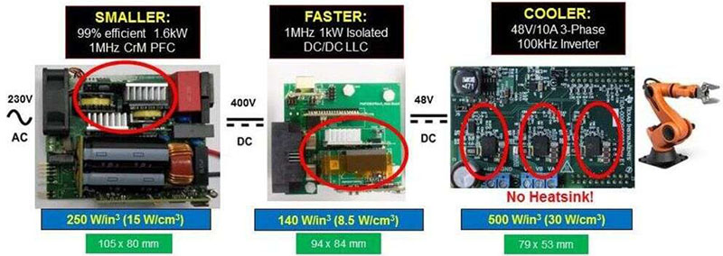 Figure 1: AC to motor power conversion
To get a better idea of the advantages of GaN technology over silicon devices, consider the transistor shown in Figure 2. First, the gate capacitance on the input is about four times lower than for a comparable silicon-based solution, yielding a higher switching rate and higher efficiency as a result of reduced gate drive losses. Another important benefit is low-output capacitance/charge, which results in higher switching frequencies and thereby helps to reduce switching losses. Additionally, RDS(on) is about two times lower than for silicon devices, resulting in lower conduction losses. Finally, use of this transistor lets us eliminate the integrated “body” diode, meaning we can achieve less ringing on switch nodes and eliminate any reverse recovery loss.
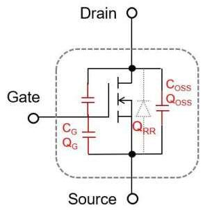 Figure 2: Key advantages of GaN over silicon solution
Integrated Driver And Protection Circuits
Texas Instruments fully integrates drivers in its GaN devices to reduce the PCB footprint and simplify the overall design. A fully integrated GaN power device such as the LMG3410 includes low switch node ringing (100-V/nanosecond switching with near-zero Vds ringing) to reduce electromagnetic interference (EMI), overcurrent protection rated for less than 100 ns, and overtemperature shutdown. A discrete GaN device requires external driver and protection circuits, which means additional costs, a larger area consumed on the PCB, and significant design challenges. Figure 3 summarizes the benefits of a device with an integrated driver compared with a discrete GaN device.
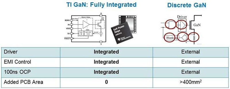 Figure 3: An integrated driver offers several benefits over a discrete GaN solution.
The driver bias voltage is the first aspect to be carefully evaluated since it is critical to both performance and long-term device reliability. As Figure 4 shows, GaN bias voltage should be tuned to maintain the mean time to failure (MTTF) to a safe value (that is, above the dashed horizontal line, corresponding to a lifetime of 10 years).
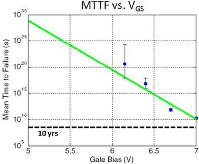 Figure 4: MTTF versus gate-to-source voltage (V(GS))
A discrete GaN also requires an appropriate overcurrent protection circuit. The design of a robust overcurrent protection circuit at a high frequency and slew rate is difficult and costly. Parasitic inductance causes switching loss, ringing, and reliability issues, especially at high GaN frequencies. With an integrated driver, it is possible to achieve a signal shape like that shown in Figure 5. The switching time is minimal, with a rise time of 102 V/ns. That means the signal rises from 0 to 400 V in less than 4 ns.
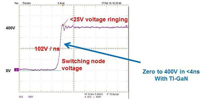 Figure 5: Switching time of a TI GaN device
External overcurrent protection (OCP) and shoot-through protection circuits also require an additional sense resistor. A resistor with a high value might be chosen to achieve a better signal-to-noise ratio (SNR). Consequently, power loop and power losses will both increase because the voltage derivation over time (dV/dt) will be lower, dropping from 100 to 80 V/ns, and because of the sense resistor. A comparison between a fully integrated and custom implemented overcurrent protection circuit is summarized in Figure 6, which also shows an example of a resistive shunt obtained with the parallel of two 12-mΩ resistors.
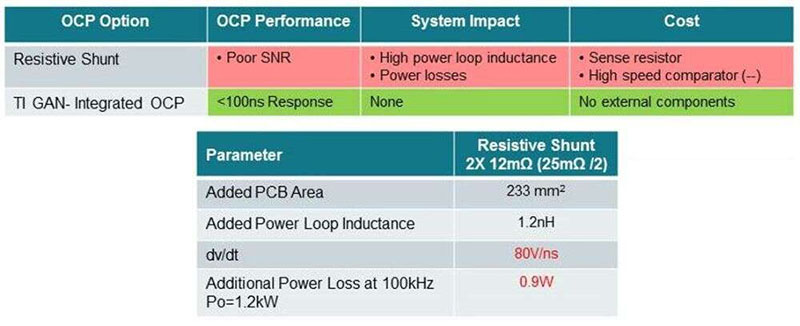 Figure 6: Integrated versus external OCP and shoot-through protection
GaN Application: AC/DC Converter
A widespread GaN application is AC/DC conversion. Figure 7 illustrates a typical topology used for implementing power supply units (PSUs) in industrial, medical, telecom, and server applications. The converter features a PFC stage with a wide input voltage (85 to 265 VAC), a constant output of 400 VDC, and an LLC converter able to provide different output voltages (12, 24, and 48 VDC).
 Figure 7: A typical application of GaN devices is the AC/DC converter.
The PFC stage of the converter can be implemented according to the schematics on the left of Figure 8, showing a typical totem-pole configuration in which a 600-V GaN half-bridge or a G3410 can be used. The PFC inductor is used to regulate input current in phase with the input voltage. The right side of Figure 8 shows the schematics for the LLC circuit, in which the resonance is determined by the value of Lr, Cr, and Lm. This stage can be implemented using GaN devices, such as the LMG5200, a high-voltage direct-drive GaNFET that provides fast switching and minimizes dead-time between half-bridge switches.
 Figure 8: Schematics of PFC and LCC stages
This solution provides high efficiency, reduces losses up to 36%, and achieves higher power density (up to 3× in totem-pole PFC versus silicon). It also allows the use of fewer heat sinks and smaller conductors and capacitors, thereby reducing the weight of the complete solution without increasing its cost.
Consider the 1.6-kW totem-pole PFC shown in Figure 9. This solution achieves an output power of 1 kW, switching frequency up to 140 kHz, output voltage of 285 VDC (derived from a wide input voltage), and power density of roughly 10 W/cm3.
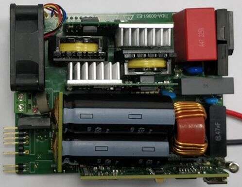 Figure 9: Totem-pole PFC using an LMG3410 GaN device
As the transistor in Figure 2 demonstrated, low output capacitance (COSS) is significant because it reduces dead time, increasing the time during which current is delivered to the output. That also means larger magnetizing inductance and lower circulating current losses as well as lower transformer fringe-field losses. Gate driver losses can be reduced as well, whereas system optimization is achievable through increases in switching frequency, efficiency, and power density. Figure 10 illustrates the relevant waveforms, showing that the switching frequency (fSW) is lower than the resonance frequency (fR). Reductions are evident in both dead time and circulating current losses.
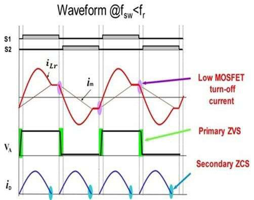 Figure 10: Reduction of dead-time between half-bridge switches
Texas Instruments’ PMP20637, shown in Figure 11, is a high-efficiency, high-power–density, lightweight resonant converter (LLC) reference design. It converts a 380- to 400-V input to a 48-V/1-kW output with a fixed 1-MHz switching frequency. The PMP20637 power stage achieves a peak efficiency higher than 97% and a power density of around 8.5 W/cm3.
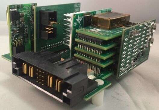 Figure 11: TI PMP20637 reference design
A comparison between GaN and silicon power MOSFET device efficiency is provided in Figure 12. As the graph shows, the reduced capacitance and circulating currents dramatically improve the efficiency at low current load. A limited resistance helps to achieve a slight improvement in efficiency at higher currents as well.
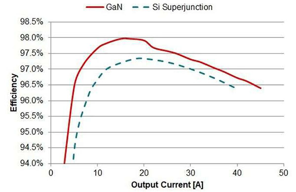 Figure 12: Efficiency comparison of GaN and silicon MOSFET devices
GaN Application: Motor Drive
GaN devices offer significant advantages in motor drive applications. Heat sinks can be reduced or eliminated. GaN also reduces or eliminates switch node oscillations, resulting in lower radiated EMI and thereby eliminating the need for an additional snubber network. Pulse-width modulation (PWM) frequency can also be increased using GaN devices, allowing the driving of very low-inductance permanent-magnetic motors or brushless DC motors. A more accurate positioning in servo drives/steppers can be obtained through minimum torque ripple, and a better sinusoidal voltage with a frequency above 1 to 2 kHz is possible — an ideal solution for high-speed drone motors.
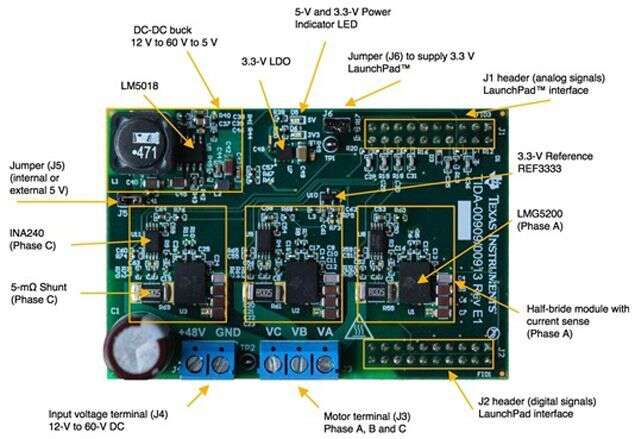 Figure 13: GaN 3-phase inverter for high-speed motors
Figure 13 shows a 48-V/10-A three-phase inverter for high-speed motors. It includes three LMG5200 GaN half-bridges. The inverter accepts a wide input voltage range (12 to 60 VDC/400 W) and has a switching frequency of 100kHz, peak efficiency of 98.5%, and power density of 9.5W/cm3.
The temperature profile shown in Figure 14 sheds light on the thermal performance of our 48-V/10-A inverter. As the figure makes clear, no heat sink is required; all the heat is dissipated by natural convection. With an external temperature of 28°C and the device switching at 100 kHz under full load conditions, a maximum temperature of 106°C is reached.
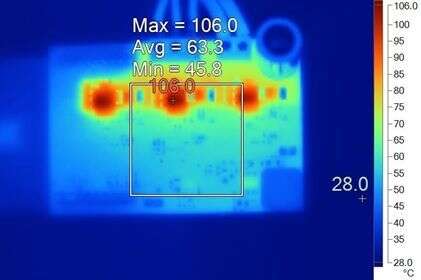 Figure 14: Thermal performance of a 48-V/10-A inverter containing three LMG5200 GaN half-bridges
TAKING GaN BEYOND 600 V
Siemens has developed a demo project for a high-efficiency grid link based on the LMG3410R050 GaN device (Figure 15). A multi-level bidirectional GaN converter transforms a three-phase grid power (400 VAC line to line and 230 VAC line to neutral) into a 700-VDC voltage. The LMG3410 with 50-mΩ RDS(on) is rated for a maximum power of 10 kW, bidirectional. A Delfino dual-core microcontroller from Texas Instruments controls the power solution and also features a Wi-Fi SimpleLink connection.
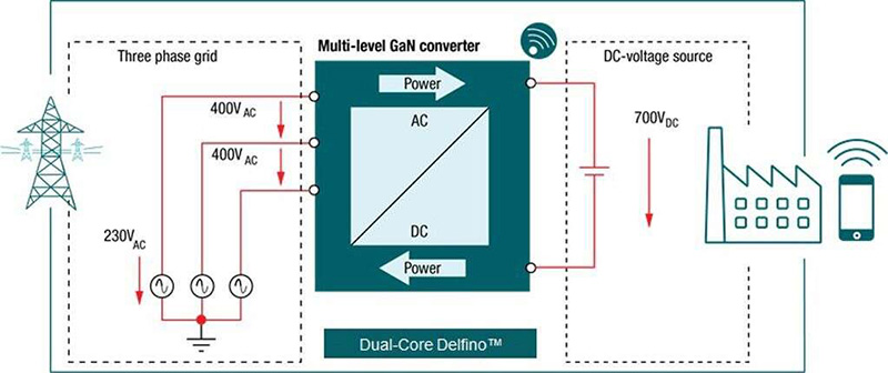 Figure 15: Efficient grid link based on the LMG3410R050
This demo application demonstrates how GaN devices offer a scalable grid solution for power applications up to 10 kW and beyond, achieving a 5× reduction in the magnetics and a 3× reduction in power components compared with a silicon design. It also represents a cloud-enabled solution for telemetry, control, and system maintenance. Further target applications, all involving power devices, are summarized in Figure 16.
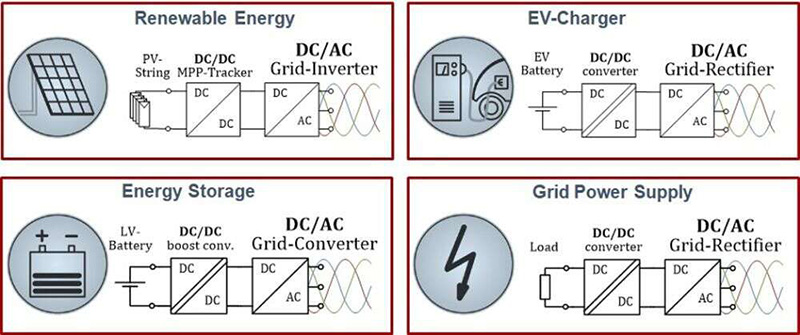 Figure 16: Other target applications for GaN devices
GaN technology is enabling a new generation of power conversion designs that would not otherwise be possible. Power density can be improved up to 3× from AC to the point of load. In an isolated LLC converter operating at a switching frequency of 1 MHz, GaN technology enables a 6× reduction in the magnetics’ size and weight. Integration of the driver and GaN in a low-inductance package provides an optimal solution for fast (higher switching frequency) and reliable (longer lifetime) devices.
By M. Di Paolo Emilio, based on a presentation by Xaver Arbinger, Senior Analog Field Application Engineer at Texas Instruments