Alex Lidow PhD, CEO, Efficient Power Conversion Corporation
For the past three decades, power management efficiency and cost have shown steady improvement as innovations in power MOSFET structures, technology, and circuit topologies have paced the growing need for electrical power in our daily lives. In the last few years, however, the rate of improvement has slowed as the silicon power MOSFET has asymptotically approached its theoretical bounds.
Silicon Power MOSFETs – The 30 Year Journey
Power MOSFETs first started appearing in 1976 as alternatives to bipolar transistors. These majority carrier devices were faster, more rugged, and had higher current gain than their minority-carrier counterparts. As a result, switching power conversion became a commercial reality. AC-DC switching power supplies for early desktop computers were among the earliest volume consumers of power MOSFETs, followed by variable speed motor drives, fluorescent lights, DC-DC converters, and thousands of other applications that populate our daily lives.
One of the earliest power MOSFETs was the IRF100 from International Rectifier Corporation, introduced in November 1978. It boasted a 100V drainsource breakdown voltage and a 0.1 Ω on-resistance; the benchmark of the era. With a die size over 40 mm2, and with a $34 price tag, the product was not destined to broadly replace the venerable bipolar transistor immediately.
Many generations of power MOSFETs have been developed by several manufacturers over the years. Benchmarks were set, and fell, every year or so for 30 plus years. As of the date of this writing, the 100 V benchmark is arguably held by Infineon with the IPB025N10N3G. In comparison with the IRF100’s figure of merit of 4 Ω – mm2, the IPB025N10N3G has an FOM of less than 0.1 Ω – mm2. 1 That is almost at the theoretical limit for a silicon device2.
There are still improvements to be made. For example, CoolMOS devices and IGBTs have achieved conductivity improvements beyond the theoretical limits of a simple vertical majority carrier MOSFET. These innovations may still continue for quite some time and will certainly be able to leverage the low cost structure of the power MOSFET and the well-educated base of designers who, after many years, have learned to squeeze every ounce of performance out of their power conversions circuits and systems.
The GaN Journey Begins
HEMT (High Electron Mobility Transistor) GaN transistors first started appearing in about 2004 with depletion-mode RF transistors made by Eudyna Corporation in Japan. Using GaN on silicon carbide substrates, Eudyna successfully brought into production transistors designed for the RF market3. The HEMT structure was based on the phenomenon first described in 1975 by T. Mimura et al4 and in 1994 by M. A. Khan et al5, which demonstrated unusually high electron mobility near the interface between an AlGaN and GaN heterostructure interface. Adapting this phenomenon to Gallium Nitride grown on Silicon Carbide, Eudyna was able to produce benchmark power gain in the multi-gigahertz frequency range. In 2005, Nitronex Corporation introduced the first depletion mode RF HEMT transistor made with GaN grown on silicon wafers using their SIGANTIC® technology7.
GaN RF transistors have continued to make inroads in RF applications as several other companies have entered in the market. Acceptance outside this market, however, has been limited by device cost as well as the inconvenience of depletion mode operation.
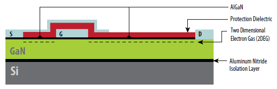
Figure 1: GaN on silicon devices have a very simple structure similar to a lateral DMOS device and can be built in a standard CMOS foundry
In June 2009 Efficient Power Conversion Corporation (EPC) introduced the first enhancement mode GaN on silicon power transistors designed specifically as power MOSFET replacements. These products were designed to be produced in high volume at low cost using standard silicon manufacturing technology and facilities. The structure is relatively simple as shown in figure 1.
Breaking Down the Barriers
The 30 year silicon power MOSFET journey taught us that there were four key variables controlling the adoption rate of a disruptive technology.
- Does it enable significant new capabilities?
- Is it easy to use?
- Is it VERY cost effective to the user?
- Is it reliable?
In the next few sections we will examine the readiness of GaN on silicon power transistors to disrupt the dominant silicon power MOSFET based on each of these four criteria. We will then go even further to look at near-future developments and speculate on their impact on the power conversion industry.
New Capabilities Enabled by GaN Power Transistors
The most significant new capabilities enabled by enhancement mode GaN HEMT devices (eHEMT) stem from the disruptive improvement in switching performance and overall device bandwidth (see Figure2). GaN also has a much higher critical electric field than silicon which enables this new class of devices to withstand much greater voltage from drain to source with much less penalty in onresistance.
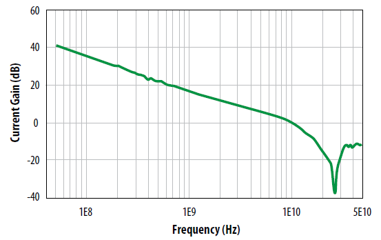
Figure 2: Gain vs Frequency for an EPC enhancement mode GaN power transistor
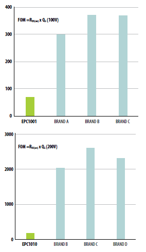
Figure 3: RQ Product for 100V and 200V benchmark silicon compared with GaN
In power MOSFETs there is a basic tradeoff between the conductivity of a part and the amount of charge required to take the device from the ON to the OFF state (Or from the OFF to the ON state). From this tradeoff comes the figure of merit called RQ product. This is defined as a device’s on-resistance multiplied by the total charge that must be supplied to the gate to switch the device at operating voltage and current. Improvements in this product have been shown to translate into improved conversion efficiency in high frequency DC-DC converters. The absolute value of RQ is also indicative of the minimum pulse widths achievable in a practical circuit. Whereas there have been great improvements in RQ product over the last several years, silicon cannot come close to the figure of merit achieved in first-generation eHEMT devices already on the market. Figure 3 shows a comparison between benchmark silicon devices and GaN devices rated at 100V and 200V.
DC-DC Converters
The ability to switch quickly and without a lot of power loss means users can go to much lower pulse widths in power conversion circuits. One significant new application needing this capability is non-isolated DC-DC converters. The basic limitation of silicon power MOSFETs has restricted single-stage, non-isolated buck converters to a practical maximum ratio of input voltage to output voltage of 10:1. Beyond that ratio, the short pulse widths required of the top transistor in the buck circuit result in unacceptably high switching losses and consequently low conversion efficiency. GaN transistors completely reset this performance bar as indicated in figures 4 and 5.
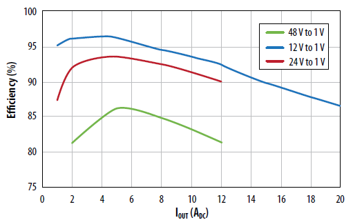
Figure 4: Buck converter efficiency vs current for various input voltages. This converter was made with a single 100V EPC1001 both as the top and bottom transistor. Ratios greater than 10:1 are generally considered impractical with silicon devices
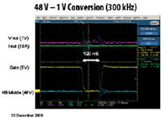
Figure 5a: 48V-1V conversion at 300 kHz using EPC1001 transistors in a buck topology
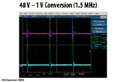
Figure 5b: 48V-1V conversions at 1.5 MHz
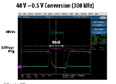
Figure 5c: 48V-0.5V conversion
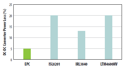
Figure 6: Power loss at 5A and 600 kHz with Vin=12V and Vout =1V of three popular point-of-load converters compared with a converter made with EPC1014/EPC1015 GaN transistors.
In addition to the added V
IN/V
OUT range made possible by GaN, existing buck converters can greatly reduce switching losses at any V
IN/V
OUT. A comparison for 12 V - 1 V converters showing this significant improvement is shown in figure 6.
AC-DC conversion, synchronous rectification, and power factor correction are all candidates for major performance improvement as new GaN transistors rapidly cover the current and voltage range of today’s power MOSFETs and IGBTs.
Class D Audio
Class D audio amplifiers have always faced the trade off between cost, size, and sound distortion.
The most significant contributors to distortion are dead time and phase shift of the output filter.
There are three distinct modes of operation which alter output pulsewidth based on deadtime. Positive inductor current, where commutation is based on the high side switch, Negative inductor current, where commutation is based on the low side switch, and bipolar current, where commutation is based on each switch. These place the deadtime at the rising edge, the falling edge, or none at all. The length of the deadtime determines the distortion for which this phenomenon is responsible. Finite switching speed and body diode forward voltage add to this effect. Enhancement mode GaN transistors have very low gate charge which translates into very short delay times and very fast switching speeds. The precision of switching allows for much better control of the switching event, and therefore enables shorter deadtime, leading to lower distortion.
The size of the output filter and the gain of the feedback are determined by the switching frequency. At low frequency, high value filter capacitors and inductor must be used to sufficiently remove the carrier frequency from the desired signal. Large value filter elements not only add cost and size to the amplifier, they also cause a phase shift. This decreases the stability of the system and limits the gain of the feedback used to compensate many of the components of distortion, thus limiting the fidelity of the system. With traditional silicon MOSFETs, frequencies are limited because power dissipation rises rapidly due to high switching losses.
GaN transistors offer both low RDS(ON) and low Gate Charge (QG) which enables excellent efficiency well into the multi-megahertz range. Amplifiers can then use lower value filter elements which reduce their cost, size, and distortion, as well as allowing higher gain feedback to reduce the switching amplifier’s contribution to the distortion.
Enhancement mode GaN transistors therefore hold the promise for both significantly higher fidelity and lower cost in Class D applications.
Are Enhancement Mode GaN Transistors Easy to Use?
How easy a device is to use depends on the skill of the user, the degree of difficulty of the circuit under development, how different the device is compared with devices within the experience of the user, and the tools available to help the user apply the device
The new generation of enhancement mode GaN transistor is very similar in its behavior to existing power MOSFETs and therefore users can greatly leverage their past design experience. Two key areas stand out as requiring special attention: relatively low gate dielectric strength (and finite gate leakage on the order of micro Amperes per millimeter of gate width) and relatively high frequency response. The first of these two differences, relatively low gate dielectric strength, will be improved as the technology matures. In the mean time, measures need to be taken to eliminate workplace ESD and to design circuits that maintain the VGS below the maximum limits in the data sheet8. The second difference, relatively high frequency response, is both a step function improvement over any prior silicon devices, and an added consideration for the user when laying out circuits. For example, small amounts of stray parasitic inductance can cause large overshoot in the gate-to-source voltage that could potentially damage devices.
On the other hand, there are several characteristics that render these devices easier to use than their silicon predecessors. For example, the threshold voltage is virtually independent of temperature over a wide range8, and the on-resistance has a significantly lower temperature coefficient than silicon8,9.
GaN transistors are also able to operate successfully at temperatures as high as 300˚C, but solder connections to the printed circuit board prevent practical application much above 125˚C. The first commercial enhancement mode parts are therefore characterized only up to 125˚C.
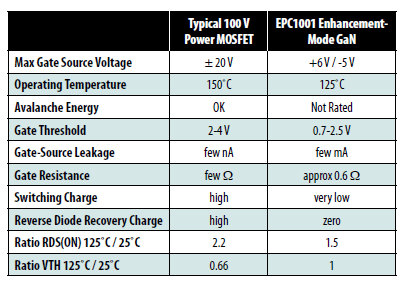
Table 1
Table 1 shows a more complete comparison between a silicon power MOSFET and an EPC1001 GaN transistor’s basic characteristics from the point of view of ease of use.
User-friendly tools can also make a big difference in how easy it is to apply a new type of device. EPC has developed a complete set of TSPICE device models available for user download10. Figure 7 shows a simple circuit and the comparison between actual device performance and the simulated result using the TSPICE model. Whereas more work refining these models needs to be done, the first-generation should provide reasonably reliable circuit performance predictions that can enhance the engineer’s productivity and the time it takes to get a product to market.
Application notes and design tips codify the collective experience of engineers over the years. Thousands of applications notes are available describing power MOSFET use in hundreds of applications. It will take many years for GaN users to match this body of knowledge but, becaus of the similarities between enhancement mode GaN transistors and silicon power MOSFETs, much of this work continues to apply. Applications notes teaching users to take full advantage of the extraordinary characteristics of GaN are also becoming available from multiple sources 11, 12.
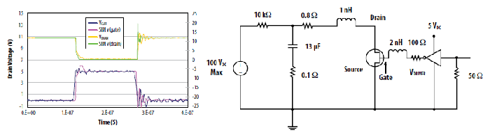
Figure 7: Circuit diagram and oscillogram comparing EPC1001 TSPICE simulation results with actual measured circuit performance
Is It VERY Cost Effective To The User?
Cost comparisons between products of different technologies can be tricky. In addition, costs are not always reflected in product prices if there is an imbalance between supply and demand. Since the market for GaN power transistors is at the very early stage of development, the most meaningful information is a cost comparison between silicon power MOSFETs and the first-generation enhancement mode transistors on the market.
The basic elements of product cost are as follows:
- Starting Material
- Epitaxial Growth
- Wafer Fabrication
- Test and Assembly
Other elements that contribute to costs such as yield, engineering costs, packing and shipping costs, and general overhead costs are assumed to be similar between the technologies for the purpose of this analysis.
Starting Material:
GaN on silicon devices are produced typically on 150mm substrates (future products will migrate to 200mm) whereas power MOSFETs are produced on anything from 100mm through 200mm substrates by the many manufacturers in this business. Because the GaN devices use standard silicon substrates, there is no cost penalty compared with power MOSFETs fabricated on similar diameter starting material. In fact, there is little cost difference per unit area between 150mm and 200mm silicon wafers and therefore we can conclude that, as far as starting material is concerned, there is no true cost difference per wafer. If you take into account the fact that the GaN device has less device area than a silicon device with similar current-carrying capability, then the cost per function is lower for GaN.
Epitaxial Growth:
Silicon epitaxial growth is a mature technology with many companies making highly efficient and automated machines. MOCVD GaN equipment is available from at least two sources, Veeco13 in the U.S. and Aixtron14 in Germany. Both make capable and reliable machines whose primary use has been the growth of GaN epitaxy used in the fabrication of light emitting diodes. None of the machines are optimized for GaN on silicon epitaxy, nor do they have levels of automation that are common on silicon machines. As a result, GaN epitaxy on silicon is significantly more expensive than silicon epitaxy today.
But this is not fundamental. Processing times and temperatures, wafer diameter, materials costs, and machine productivity are all on a fast track of improvement with no fundamental limit far away from silicon limits. Within the next few years, assuming widespread adoption of GaN as a replacement for silicon power MOSFETs, it is expected that the cost of the GaN epitaxy will approach that of silicon epitaxy.
Wafer Fabrication:
The simple structure depicted in Figure 1 is not complicated to build in a standard silicon wafer fab. Processing temperatures are similar to silicon CMOS, and cross contamination can easily be managed. Today, EPC processes all their wafers in Episil Inc., a well-established foundry in Taiwan.
There are no material differences between the cost of wafer fabrication of a GaN power device and a power MOSFET.
Test and Assembly:
In the assembly process there are significant differences favoring the cost structure of GaN on silicon devices whereas the testing costs are equivalent.
Silicon power MOSFETs need a surrounding package typically made of a copper leadframe, some aluminum, gold, or copper wires, all in a molded epoxy envelope. Connections need to be made to the top and bottom of the vertical silicon device, the plastic molding is needed to keep moisture from penetrating to the active device, and there needs to be a means of getting the heat out of the part.
Traditional power MOSFET packages such as the SO8, TO220, or DPAK add cost, electrical and thermal resistance, and increase reliability and quality risks to the product.
GaN on silicon can be used as a “flip chip” without compromise of electrical, thermal, or reliability characteristics.
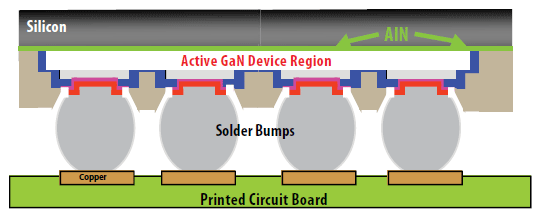
Figure 8: GaN on silicon can be used as a “flip chip”. The active device is isolated from the silicon substrate and can be completely encapsulated prior to singulation.
Referring to figure 8 you can see that the active device region is isolated from the silicon substrate much like a silicon-on-sapphire device. As a result, the active GaN device can be completely encapsulated by passivating layers. In addition, the silicon substrate can be directly attached to a heat sink for excellent thermal performance.
In short, GaN on silicon eliminates the need for a package and therefore also eliminates both the cost, wasted board space, added thermal and electrical resistance, and the most common reliability issues plaguing packaged power devices.
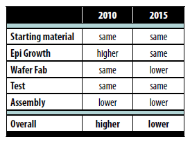
Table 2
Table 2 summarizes the cost difference between GaN on silicon compared with silicon power transistors on a per unit area basis in 2010 and as anticipated in 2015. Since GaN on silicon devices are smaller for the same function, the overall conclusion would favor GaN on silicon even more than this table shows.
Is GaN reliable?
The cumulative reliability information available on silicon power MOSFETs is staggering. Many years of work have gone into understanding failure mechanisms, controlling and refining processes, and designing products that have distinguished themselves as the highly-reliable backbone of any power conversion system. GaN on silicon transistors are just beginning this journey. Preliminary results, however, are encouraging. Nitronex has published results from their qualification tests15 and devices have been successfully applied to many RF applications with good results.
As of the date of this writing, EPC has established the basic capability of enhancement mode GaN on silicon transistors. Full reliability reports are available at https://epc-co.com/epc/design-support/gan-fet-reliability.
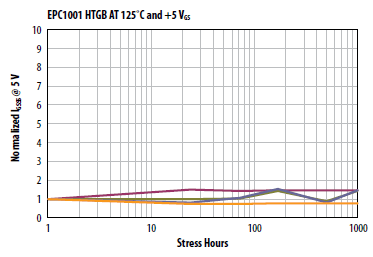
Figure 9: 1000 Hour gate stress capability at 125oC and +5Vgs
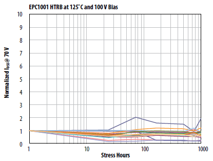
Figure 10: 1000 Hour drain-source stress capability at 125˚C and 100VDS
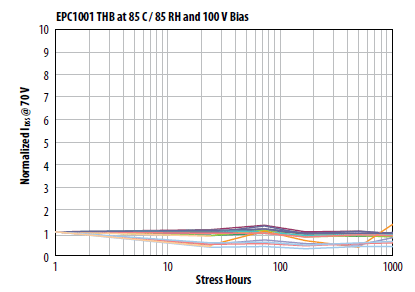
Figure 11: 1000 Hour humidity stress capability at 85% RH and 85˚C with 100VDS and no underfill
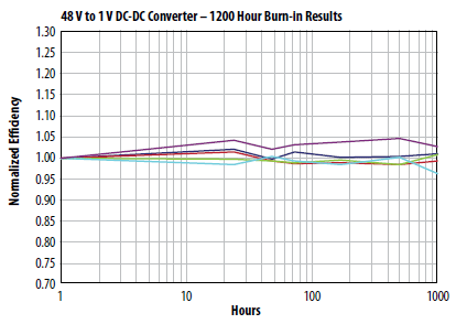
Figure 12: 1000 Hour DC-DC converter burn-in results using 2 each EPC1001 GaN transistors at 40oC ambient and 10A
Intermediate device results are shown in figures 9, 10, and 11. As can be seen, tested devices are stable after 1000 hour stresses of the gate, the drain-source, and when exposed to high humidity with bias.
EPC has also put devices into 48 V - 1 V DC-DC converters and operated them at maximum stress for 1000 hours without failure. Results shown in Figure 12.
There is much to be done to understand the various failure mechanisms associated with this new technology. All entrants into this field will hopefully contribute significantly to this body of knowledge. Nevertheless, the data we have so far suggests this technology is today capable of performing at acceptable levels of reliability in commercial applications.
The GaN journey is just beginning. There are profound improvements that can be made in basic device performance as measured by the RQ figure of merit. As we learn more about the material and the process, a factor of two improvement can be reasonably expected over the next three years and a factor of ten over the next 10 years.
We can also expect devices to emerge with much higher breakdown voltage in the near future as EPC and other companies have discussed openly their intentions in this area.16. Higher voltages for GaN transistors with undoubtedly follow and will displace silicon IGBTs and even SiC-based transistors due to the lower manufacturing costs and lower conduction losses2.
Perhaps the greatest opportunity for GaN to impact the performance of power conversion systems comes from the intrinsic ability to integrate both powerlevel and signal-level devices on the same substrate. GaN on silicon, much like SOI, has no significant parasitic interaction between components, allowing designers to easily develop monolithic power systems on a single chip.
Figures 13, 14, and 15 show various integrated devices already fabricated. Figure 13 is a three-phase motor control IC made by Panasonic17 including the IC driver on board with the six power transistors. Figure 14 is a full bridge power device from EPC, and Figure 15 is a power transistor with on-board drivers also from EPC.
In the late 1970’s the pioneers in the development of power MOSFETs believed they had a technology that would displace bipolar transistors completely. Thirty years later, we still have plenty of applications that prefer bipolar transistors over power MOSFETs but the size of the power MOSFET market is many times larger than the bipolar market largely due to all the new applications and new markets enabled by that breakthrough technology.
Today, we are at that same threshold with enhancement mode GaN on silicon. Like the power MOSFET of 1976, we are beginning an exciting journey with new products and breakthrough capabilities almost monthly.
The power MOSFET is not dead, but is nearing the end of the road of major improvements in performance and cost. GaN will most probably become the dominant technology over the next decade due to its large advantages in both performance and cost; advantage gaps that promise to widen as we quickly climb the learning curve18.