EPC9003C : 200 V Half-Bridge Development Board
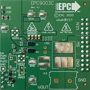
The EPC9003C development board has a 200 V maximum device voltage, 5 A maximum output current, in a half-bridge topology with onboard gate drives, featuring the EPC2010C enhancement-mode (eGaN®) field effect transistor (FET)
The purpose of this development board is to simplify the evaluation process of the EPC2010C eGaN FET by including all the critical components on a single board that can be easily connected into any existing converter.
Status: Obsolete
The GaN Experts recommend EPC90124 for new designs