Designing Manufacturable and Reliable Printed Circuit Boards Employing Chip-Scale eGaN FETs
GaN Talk – Michael de Rooij, Ph.D.
Dec 05, 2017
Written by Michael de Rooij and Alana Nakata - Efficient Power Conversion
Published in: PCIM Europe 2017; International Exhibition and Conference for Power Electronics, Intelligent Motion, Renewable Energy and Energy Management; Proceedings of
eGaN FETs, which are available in non-traditional chip scale packages (CSP) as land grid array (LGA) and/or ball grid array (BGA) formats, have repeatedly demonstrated higher power density and higher efficiency performance than equivalent MOSFETs across various applications [1, 2]. Those improvements are contingent upon proper layout practices documented extensively in [1, 3] that minimize unwanted parasitic elements. Over the seven years since eGaN FETs were first launched into the market there have been a total of 127 device failures out of a total of more than 17 billion hours in actual use in the field, 75 of which were a result of poor assembly technique or poor printed circuit board (PCB) design practices [4]. Designers are becoming more familiar with the PCB design rules that affect manufacturability and are less forgiving compared to MOSFETs due to their relatively smaller sizes. This paper will cover the various guidelines for PCB design that maximize the performance of eGaN FETs and reliability yet still rely on existing PCB manufacturing capabilities.
Printed circuit board design considerations and guidelines for eGaN FETs
 Figure 1: Soldermask defined (SMD) versus non-soldermask defined (NSMD) pad
The quality of the solder bump interfacing the eGaN FET to the PCB is crucial for a reliable electrical, thermal and mechanical connection. The factors that define this quality include its symmetry, volume, height, and finish. These factors may be overlooked by a designer primarily focused on layout, and thus the device manufacturer must take on the responsibility for providing clear and simple guidelines in their datasheets. Those guidelines include the recommended footprint (copper and soldermask) and stencil designs. For eGaN FETs and integrated circuits a soldermask defined (SMD) footprint for the LGA and BGA bumps is recommended as shown in figure 1 (right). Figure 1 (left) shows a non-soldermask defined (NSMD) footprint pad that is typically used for PCB deigns. In our investigations of failures at customers’ assembly facilities we have found instances where PCB manufacturers modified Gerber files to accommodate their internal manufacturing design guidelines developed for much larger packages. A design review prior to final board release would highlight this problem prior to incurring scrap or rework expenses in assembly. Figure 2 shows how the SMD pad works to reduce mechanical stress by ensuring a symmetrical bump after soldering. In contrast, using a NSMD footprint can result in an asymmetrical solder bump as 100% perfect registration between the copper and mask layers in not likely. In the case of the SMD footprint, immunity is ensured within the manufacturing tolerances of the PCB.
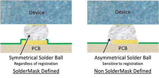 Figure 2: Effect of copper to soldermask layer registration on the solder ball symmetry
The height of the solder bump between the boards and the device is also critical for mechanical stress and has been determined to yield a balance between reliability, electrical and thermal performance. If the bump height is too low then the device will experience high thermally-induced mechanical stresses that will result in solder ball or under bump metal fatigue, while devices seated too high will experience higher electrical and thermal stresses (due to reduced heatsinking effects from the PCB) [4]. The optimal height is different for each device. For LGA and BGA devices additional options such as various solder types must also be part of the design decisions. Figure 3 shows how different solder types can yield different stencil designs.
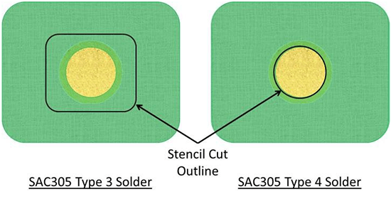 Figure 3: Impact of solder choice on stencil design
Many designers will also decide to use a hot air solder leveling finish (HASL) for the board that deposits solder on the pads. This solder deposit yields small amounts of solder on the pads that add to the amount of solder that will be dispense via the stencil and will be included in the bump, ultimately affecting the bump volume and hence its quality. In addition, the HASL process is imprecise and typically yields uneven solder on the pads of varying quantities as can be seen in figure 4 (right). This can lead to die tilt and/or open solder joint s. It is therefore recommended to use an electroless nickel immersion gold (ENIG) pad finish that yields a very uniform and flat pad as shown in figure 4 (left).
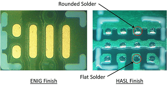 Figure 4: ENIG finish versus HASL finish showing uneven solder heights
The quality of the finished pad is key to good solderability and residual soldermask can prevent the solder from adhering to the pad. Figure 5 shows examples of a clean pad (left) versus a contaminated pad (right).
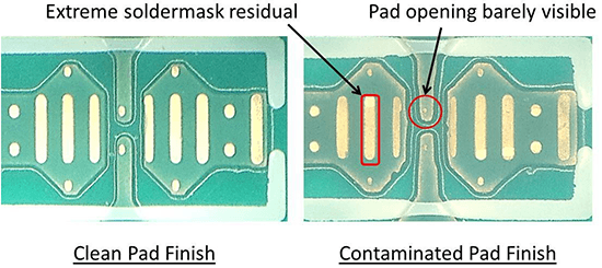 Figure 5: Examples of a contaminated pad versus clean pad
Summary
The final paper will cover many more aspects of the PCB design with examples, that impact reliability and performance such as layer registration, quality of silkscreen and its impact on solder paste dispensing, placing vias under solder pads, board bowing, soldering temperature profile, layer stackup, copper thickness, spacing requirements, stencil cuts, hole wall to hole wall spacing and more.
References
- A. Lidow, J. Strydom, M. de Rooij, D. Reusch, GaN Transistors for Efficient Power Conversion. Second Edition, Wiley, ISBN 978-1-118-84476-2.
- A. Lidow, D. Reusch, “A New Generation of Power Semiconductor Packaging Paves the Way for Higher Efficiency Power Conversion,” International Workshop on Integrated Power Packaging (IWIPP), May 2015, pp 99 – 102.
- D. Reusch, J. Strydom, “Understanding the Effect of PCB Layout on Circuit Performance in a High Frequency Gallium Nitride Based Point of Load Converter,” Applied Power Electronics Conference, APEC 2013, pp. 649–655, 16–21 March 2013.
- C. Jakubiec, R. Strittmatter, C. Zhou, “EPC eGaN® FETs Reliability Testing: Phase 8,” 2016