Why GaN in Space?
GaN Talk – Alex Lidow, Ph.D.
Jun 28, 2020
Packaged SEE Immune and Radiation Hardened enhancement mode gallium nitride (eGaN) devices offer dramatically improved performance over the aging Rad Hard silicon MOSFET, enabling a new generation of power converters in space operating at higher frequencies, higher efficiencies, and greater power densities than ever achievable before.
Radiation in Space
There are several types of radiation experienced by semiconductors in space. Devices in satellites in orbit around our earth, or in exploration satellites visiting the most distant parts of our solar system, all experience some form of high-energy radiation bombardment. Three of the primary types of radiation are gamma radiation, neutron radiation, and heavy ion bombardment.
An energetic particle can cause damage to a semiconductor in three primary ways; it can cause traps in non-conducting layers, it can cause physical damage to the crystal – also called displacement damage, or it can generate a cloud of electron-hole pairs that will cause the device to momentarily conduct, and possibly burn out in the process.
The physical properties and construction of GaN devices compared to silicon give GaN superior immunity to the damage caused by radiation in space.
Gamma Radiation
eGaN devices are built very differently from silicon MOSFETs. All three terminals of a GaN FET; gate, source, and drain, are located on the top surface. Similar to silicon MOSFETs, conduction between source and drain is modulated by biasing the gate electrode from zero volts to a positive voltage. In eGaN FETs, the gate is separated from the underlying channel by an aluminum gallium nitride layer. This layer does not accumulate charge when subjected to gamma radiation.
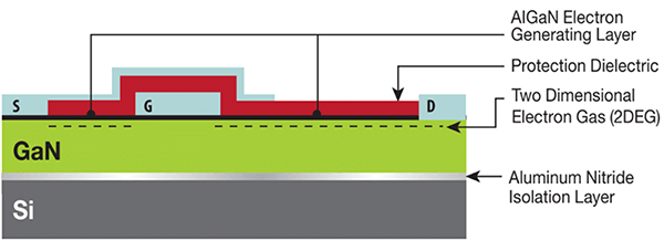 Figure 1: Cross section of a typical enhancement mode GaN (eGaN®) device
EPC Space subjected the 100 V family of eGaN transistors to 500 kRad(Si) of Gamma radiation. The leakage currents from drain to source and gate to source were measured, as well as the threshold voltage and on-resistance of the devices at various checkpoints along the way, confirming that there are no significant changes in device performance. Subsequently, devices have been taken out to 50 MRads(Si) confirming that eGaN devices will not be the first part to fail due to gamma radiation in any space system.
Neutron Radiation
The primary failure mechanism for devices under neutron bombardment is displacement damage. High energy neutrons will scatter off atoms in the crystal lattice and leave behind lattice defects. As with gamma radiation, the impact of neutrons on the GaN crystal and the entire device structure is minimal.
The reason for GaN’s superior performance under neutron radiation is that GaN has a much higher displacement threshold energy compared with silicon. In figure 2 you can see the displacement energy on the vertical axis compared with the inverse of the lattice constant for various crystals. Note how much higher the displacement energy of GaN is compared with silicon.
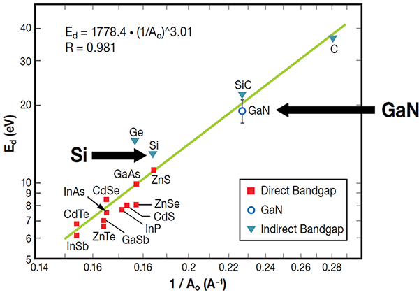 Figure 2: Displacement energy compared with the inverse of the lattice constant for various crystals
Single Event Effects
In a silicon MOSFET there are two primary failure mechanisms caused by heavy ions, single event gate rupture (SEGR) and single event burnout (SEB). SEGR is caused by the energetic atom causing such a high transient electric field across the gate oxide that the gate oxide ruptures. Whereas, SEB is caused when the energetic particle transverses the drift region of the device where there are relatively high electric fields. The energetic particle loses its energy while generating a large number of hole electron pairs. Single event burnout, or SEB is caused when the energetic particle transverses the drift region of the device where there are relatively high electric fields. The energetic particle loses its energy while generating a large number of hole electron pairs. These hole electron pairs cause the device to momentarily short circuit between drain and source. This short circuit can either destroy the device, and this is call single event burnout, or the device can survive but it appears as a momentary short circuit that can cause damage to other components in the system, called single event upset, or SEU.
Since eGaN devices do not have a gate oxide, they are not prone to single event gate rupture. Since eGaN devices do not have the ability to conduct large numbers of holes very efficiently, they are also not prone to single event upset. Shown in figure 3 is the primary failure mechanism for eGaN devices under heavy ion bombardment. The conditions are about the maximum conditions possible, with an 85 MeVcm2/mg (LET) beam of gold atoms pummeling the device biased at the maximum data sheet limit. The vertical axis is the device leakage current while the horizontal axis is the number of heavy ions absorbed by the device per square centimeter. The dotted line shows the gate-to-source leakage current, and the solid line shows the drain-to-source leakage current for three separate FBG10N30 100 V eGaN transistors. Note that the gate leakage does not go up during bombardment. The drain-source leakage, however, does start to rise as the displacement damage from the heavy ions increases, but devices stay within data sheet limits well past 106 ions/cm2.
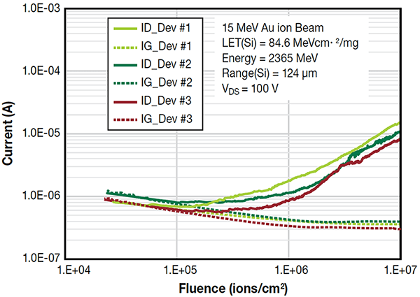 Figure 3: SEE primary failure mechanism for eGaN devices under
System Performance
It has been demonstrated that eGaN devices outperform the aging Rad Hard silicon MOSFET in radiation testing, so now we look at performance comparisons. The tables below compare the electrical performance of 100 V and 200 V Rad Hard GaN transistors against Rad Hard power MOSFETs from Infineon.
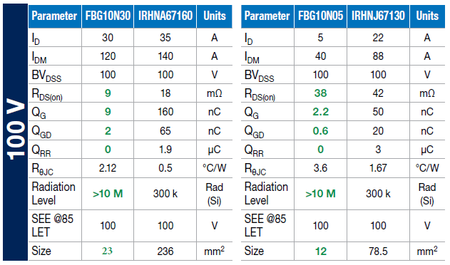
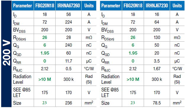 Table 1: Electrical performance comparisons Rad Hard eGaN transistors against power MOSFETs from Infineon
The 100 V FBG10N30 packaged part from EPC Space has half the on-resistance compared to the silicon MOSFET yet is one-tenth the size and has about one-twentieth the gate and gate-drain charges that determine switching speed. In addition, the radiation resistance is significantly higher.
At 200 V, the difference in electrical performance of the eGaN transistors is even greater. Note that the eGaN device listed on the left side of the 200 V section of table 1 has similar on-resistance to its MOSFET counterpart, yet is one-tenth the size, and has about 30 times better switching performance while demonstrating superior radiation resistance.
As an example of how the superior performance of GaN translates into system performance, figure 4 depicts a converter from VPT using EPC Space devices to provide a solution that increases power supply efficiency, resulting in reduced system size, weight, and cost. With up to 95% efficiency, using GaN results in greater efficiency. The converter has been designed specifically for spaceborne telecommunications where high efficiency, low noise, and radiation tolerance are imperative.
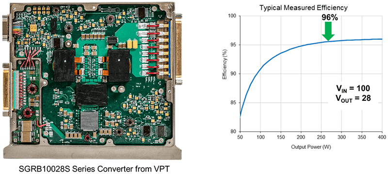 Figure 4: photo of SGRB10028S converter from VPT using EPC Space GaN devices
And the typical measured efficiency
The Future
eGaN devices have significantly different failure mechanisms compared to silicon MOSFETs and when exposed to various forms of radiation, eGaN devices are more rugged that Rad Hard MOSFETs. Equally important, the electrical performance of GaN devices is many times superior to the aging silicon power MOSFET enabling entirely new architectures for satellite power and data transmission, robotics, drones, and aeronautical power systems.
The initial SEE Immune and Radiation Hardened family of GaN power solutions from EPC Space will quickly expand to cover a myriad of mission critical applications including power management for Micro, LEO, GEO satellites as well as deep space and outer space explorations, motor drives for robotic systems used in missions, and lidar systems for precise positioning and docking.
Be sure to ‘watch this space’ – pun intended!