Reliable Assembly of PQFN GaN Devices: Practical Stencil Design Guidelines for Engineers
GaN Talk – Gerald Adriano
Aug 26, 2025
As gallium nitride (GaN) adoption accelerates in applications from data centers and robotics to automotive and consumer electronics, packaging plays an increasingly critical role. EPC’s thermally enhanced power quad flat no-lead (PQFN) packages deliver the performance and density engineers demand, but success in real-world systems depends on one thing: reliable assembly.
Unlike ball grid array (BGA) packages, PQFN devices have lower solder stand-off heights. This makes stencil design, solder paste transfer, and stand-off consistency crucial to ensure both mechanical robustness and long-term thermo-mechanical reliability. To address this, EPC engineers developed an application note, AN029: Solder Stencil Design Guidelines for Reliable Assembly of PQFN GaN Devices, which distills extensive experimental data into practical rules for assembly engineers.
This blog post summarizes key takeaways from that application note and provides engineers with actionable stencil design rules to maximize the performance and reliability of GaN-based systems.
Why Stencil Design Matters for PQFN GaN Devices
PQFN packages are favored for their compact footprint, low parasitics, and excellent thermal performance. However, these benefits also mean that solder stand-off heights are lower than in legacy BGA and LGA packages.
A well-designed solder stencil directly impacts:
- Stand-off height – ensuring mechanical clearance and consistent joint formation.
- Die tilt – minimizing stress during temperature cycling.
- Reliability – improving long-term thermal and mechanical endurance.
EPC’s guidelines are based on first principles and validated by extensive cross-sectional SEM analysis, providing engineers with confidence that following them will yield predictable, repeatable outcomes.
Key Parameters in Stencil Design
1. Aspect Ratio
- Defined as aperture width ÷ stencil thickness

- Must be greater than 1.5 for acceptable solder paste release.
- Ratios below 1.5 increase paste adhesion to the aperture wall, reducing transfer efficiency.
2. Area Ratio
- Defined as aperture opening area ÷ aperture sidewall area.
&
- Must be greater than 0.66 (per IPC-7525A standards).
- Larger area ratios improve transfer efficiency and reduce variation.
3. Transfer Efficiency
- The ratio of solder volume deposited on the pad to the theoretical aperture volume.

- Influenced by stencil fabrication (laser cut vs. etched), aspect ratio, and area ratio.
- Higher transfer efficiency means more consistent stand-off heights and fewer voids
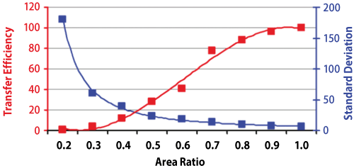 Figure 1: Transfer efficiency vs. area ratio and standard deviation
Case Studies
1. EPC23102 ePower™ Stage IC
- Package: 3.5 × 5 mm PQFN, 100 µm stencil.
- Predicted stand-off heights: 46–57 µm across different pad geometries.
- Measured values: 48–57 µm, within ±2–5 µm of prediction.
- Package tilt measured ≤ 5 µm, confirming uniform solder distribution
2. EPC2302 Enhancement-Mode GaN FET Package: 3 × 5 mm PQFN, 150 µm stencil
- Package: 3 × 5 mm PQFN, 150 µm stencil.
- Predicted stand-off heights: 76–81 µm.
- Measured values: 76–81 µm, confirming model accuracy.
- Tilt between opposite pads: ≤ 5 µm, validating stencil rule effectiveness
The close agreement between predicted and measured solder stand-off heights validates the stencil design methodology. Key implications for engineers include:
- Predictability: Stand-off height can be estimated analytically before assembly.
- Consistency: Following area and aspect ratio rules ensures minimal tilt and reliable mechanical bonding.
- Reliability: Improved thermo-mechanical performance under thermal cycling.
- Scalability: Applicable across both integrated power stages and discrete devices.
These guidelines minimize trial-and-error in stencil design, accelerating time-to-market for GaN-based systems.
Conclusion
EPC’s PQFN packaging delivers the performance, density, and manufacturability needed for next-generation power systems, but long-term success ultimately depends on reliable assembly. Application Note AN029 provides engineers with a clear, experimentally validated framework for stencil design. By applying these guidelines, designers of motor drives, converters, and other high-density systems can achieve predictable stand-off heights, minimal device tilt, and improved thermal cycling reliability. In doing so, AN029 offers not just practical stencil design rules, but a first-principles toolset that enables confident integration of GaN into production-ready products.
Next Steps and Resources
Download the full application note for detailed formulas, design rules, and experimental data: AN029 – Solder Stencil Design Guidelines for Reliable Assembly of PQFN GaN Devices
Ask a GaN Expert
Have questions about PQFN assembly, layout practices, or device selection? EPC engineers are ready to help. Ask a GaN Expert
GaN First Time Right
Access reference designs, layout checklists, and design support tools to ensure your first GaN design is a success. GaN First Time Right
Explore Demonstration Boards
Accelerate prototyping and validation with EPC’s family of demonstration boards featuring PQFN-packaged GaN devices. View Demonstration Boards