EPC’s GaN Roadmap Comes Into Focus Ahead of PCIM Asia: Gen 8 and Trinity Point to the Next Power-Density Leap
GaN Talk – Maurizio Di Paolo Emilio
Aug 19, 2026
As AI infrastructure, humanoid robots, drones, autonomous machines and space systems push power electronics toward higher efficiency and power density, gallium nitride (GaN) is moving into increasingly demanding applications. At PCIM Asia 2026 in Shenzhen, Efficient Power Conversion (EPC) will showcase its latest GaN technology while offering a preview of where the company believes the technology is heading next.
The event, taking place August 26–28, will be particularly relevant for designers working on AI power delivery and intelligent motion systems. EPC will demonstrate its GaN portfolio across the power-conversion chain, from 800 VDC distribution to point-of-load conversion, while its roadmap points toward two developments with potentially broader implications: Gen 8 GaN for ultra-high-frequency, low-voltage power conversion and Trinity, EPC’s approach to highly integrated GaN motor drives.
From 800 VDC to the point of load
The rapid evolution of AI servers is changing the architecture of data-center power delivery. As rack power moves toward the megawatt range, traditional multi-stage architectures face increasing losses, thermal constraints and physical limitations.
EPC CEO Alex Lidow observes that the transition to an 800 VDC rack-level bus is a fundamental architectural shift.
“The minute you go directly to 800 volts to the rack, GaN becomes essential to efficiently convert the power from 800 V all the way down to the point of load.”
The challenge is not simply converting 800 V to a lower intermediate voltage. Increasing GPU currents are making the final power-delivery stages increasingly difficult. With GPU rails moving toward approximately 0.5–0.6 V, and requiring thousands of amperes current, even very small parasitic resistances can produce significant losses.
Lidow points to the resulting need to move conversion physically closer to the processor:
“You’ve got to locate your power supplies right underneath the GPUs, as close as possible connected up underneath, and that means that needs to be very thin, and it also needs to have the greatest span of voltage. This is not a new insight, but only with GaN can you bring relatively high voltages, such as 6 V, right to the final conversion stage.”
This is where EPC's GaN technology becomes central to the architecture: high-frequency switching can reduce the size of magnetics and passives while extremely low conduction losses help address the efficiency challenge at high currents while eliminating costly and inefficient intermediate conversion steps using low voltage IVRs (Integrated Voltage Regulator).
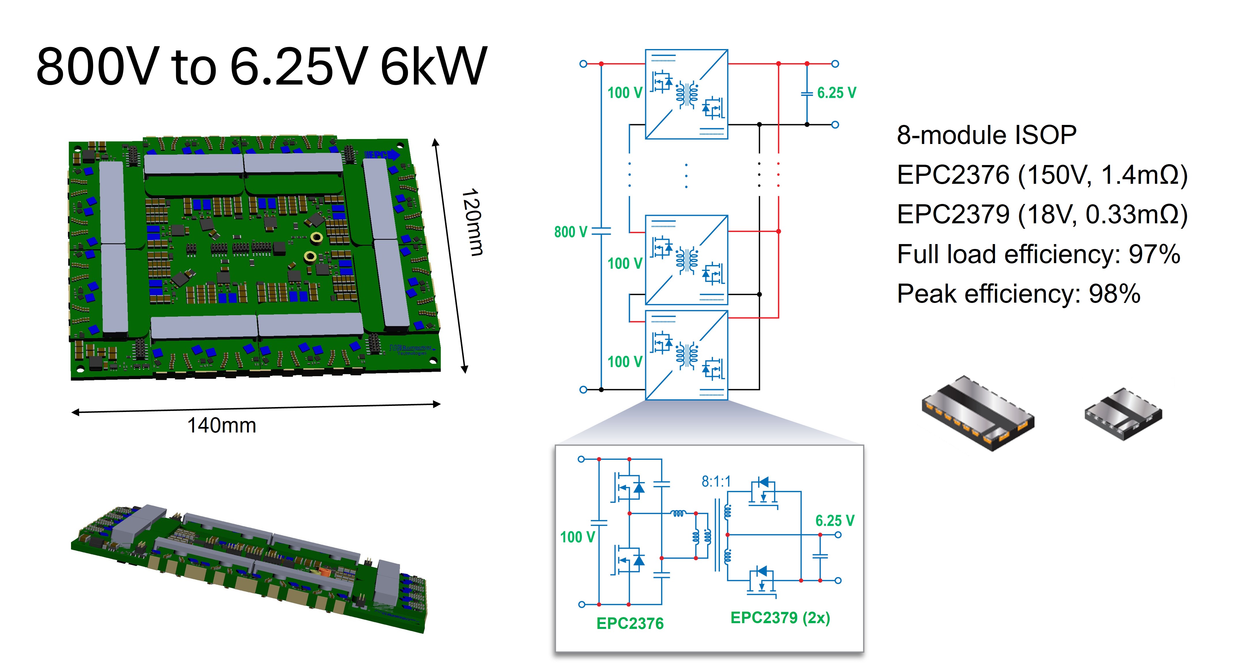
Figure 1: 800V to 6.25V, 6kW Board
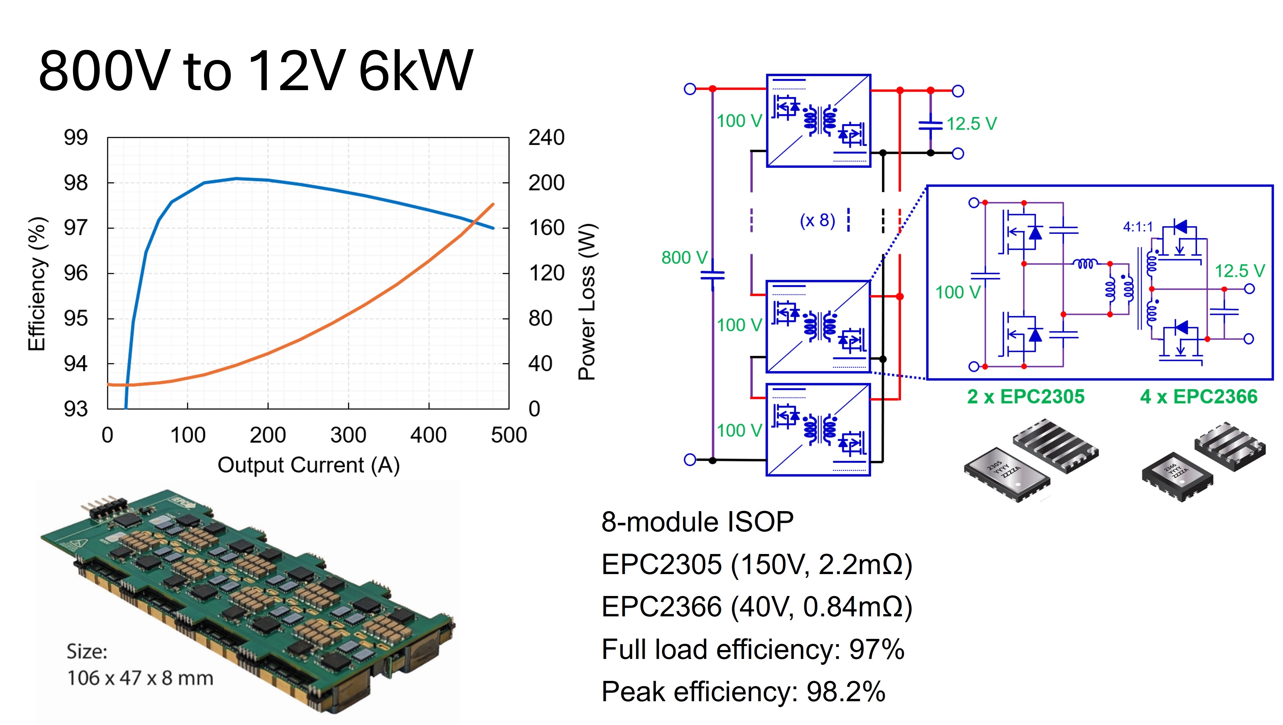
Figure 2: 800V to 12V, 6kW Board
The megawatt-rack challenge
Moving to megawatt-class racks creates another fundamental problem: there is simply less physical space available for power electronics.
According to Lidow, increasing server density can reduce the spacing between boards dramatically. With conventional airflow no longer sufficient, liquid cooling becomes necessary, introducing cooling plates and additional mechanical constraints.
“The challenge becomes fitting all your power electronics in a very thin space, and not only that, but you've got these incredible amounts of current, which, if you want to conduct them efficiently, requires thick things like thick copper and thick transformers and thick everything.”
The architectural objective therefore becomes a balance between eliminating conversion stages and controlling distribution losses.
An 800 V-to-6 V architecture, for example, can reduce the number of stages, but distributing 6 V over significant distances creates substantial current and conduction losses. The answer is to bring the conversion stage extremely close to the GPU.
“That all takes GaN,” Lidow says. “You have to go to very high frequencies to keep everything as thin and small as possible.”
This combination of high voltage, high current, high frequency and extreme power density is becoming one of the strongest arguments for EPC's GaN technology in AI infrastructure.
Gen 7 opens the low-voltage GaN market
While the High voltage AC to 800 V side of the architecture naturally involves high-voltage devices using SiC in the front end, EPC sees a rapidly expanding role for GaN as soon as the voltage reaches the back of the server rack.
The company's Gen7 technology is particularly important because it extends the performance advantage of GaN into voltage ranges traditionally dominated by silicon MOSFETs.
“Before our seventh-generation platform, gallium nitride transistors really were much more efficient than silicon above 40 volts. But with Gen 7, now GaN is much more efficient than silicon below 40 volts.”
This creates a significant opportunity in AI power systems, where large amounts of power are ultimately delivered through 48 V, 12 V, 6 V and sub-1 V domains.
The company's low-voltage portfolio is therefore becoming increasingly important as AI architectures move toward higher rack voltages and lower processor voltages.
Gen 8: beyond the IVR architecture
The next step is Gen 8.
EPC has introduced the concept of an eighth-generation GaN platform aimed specifically at low-voltage, high-frequency and high-power-density applications. The architecture targets direct conversion from approximately 6.25 V to sub-1 V processor rails at multi-megahertz switching frequencies.
The potential impact goes beyond incremental efficiency improvements.
“With gallium nitride, we can get, for example, from 6 volts down to 0.6 volts with very high efficiency and at frequencies as high as 10 megahertz. This eliminates the need for an IVR stage.”
The advantages are both electrical and mechanical: fewer stages, shorter current paths, smaller magnetics and potentially a much thinner power-conversion solution.
EPC's Gen 8 concept therefore represents an important shift in the role of EPC's GaN technology - from a high-performance switching device to an enabling technology for a new power architecture.
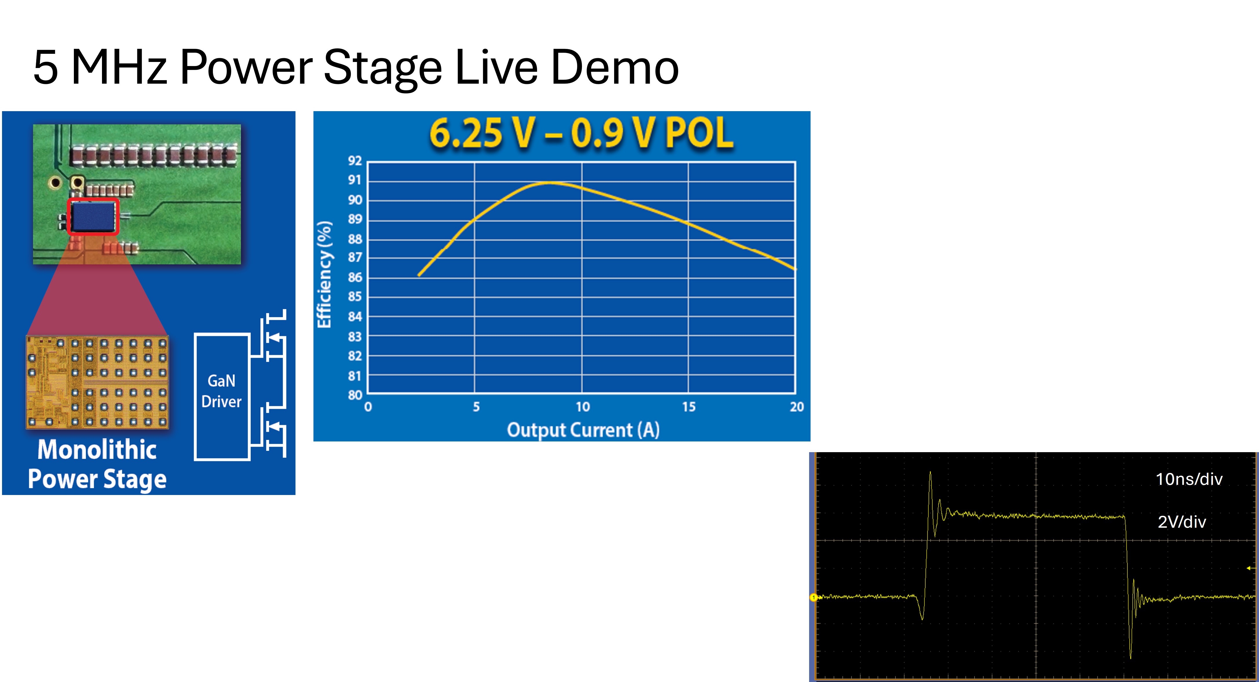
Figure 3: 5 MHz Power Stage
GPU power is becoming a current problem
The scale of the challenge becomes clearer when looking at processor power.
Lidow points out that the evolution of GPU generations is driving current requirements dramatically higher. A GPU operating at thousdands of watts and approximately 0.5–0.6 V requires thousands of amperes.
“Now we're getting into the Vera Rubin generation, which will be over 4,400 watts at 0.6 V, so we're talking about close to 10,000 amperes.”
The consequence is that milliohms of resistance are no longer a minor design consideration.
“If you have a micro ohm of resistance in the line at 10,000 amps, you're dissipating about 100 W, or about two percent of your power right there.”
This is why power conversion must move closer to the processor and why the voltage range of the final converter becomes so important.
According to Lidow, the future intermediate-voltage regulator is therefore less likely to be a traditional 1.8 V-to-0.6 V or 3.3 V-to-0.6 V converter and increasingly a 6 V-to-0.6 V GaN converter positioned extremely close to the GPU.
Trinity targets the next generation of motion control
The other technology to watch is Trinity, which addresses a very different but equally demanding problem: motor control.
Humanoid robots can contain dozens of motors, from large joints to highly compact actuators in hands and fingers. Every gram, cubic millimeter and watt matters. GaN’s ability to switch at high frequency and operate efficiently at typical 48–60 V motor-bus voltages makes it particularly attractive for these systems.
EPC has progressively integrated its motor-drive technology, moving from discrete GaN devices to half-bridge modules and then to three-phase solutions. The EPC33110, for example, integrates three GaN half-bridges and gate drivers in a compact package for brushless DC (BLDC) motor applications, supporting up to 80 V input, PWM operation up to 100 kHz and up to 20 ARMS per phase.
Trinity takes that integration philosophy another step.
Trinity integrates all three motor phases onto a single GaN chip in a 3.3 x 3.3 mm QFN package, turning the motor power stage into a highly compact building block that can be connected to the controller and sensors.
The significance extends beyond size.
GaN’s zero reverse-recovery characteristic allows designers to reduce dead time substantially compared with conventional silicon MOSFET motor drives. Higher switching frequency can also reduce the size of passive components, eliminates electrolytic capacitors, while improved dynamic response can be valuable in applications where precise torque and rapid movement are essential.
For humanoid robots, that translates into smaller actuator electronics, reduced weight and greater mechanical integration. For drones and e-bikes, the same characteristics contribute to longer operating time and improved power density.
GaN and the rise of autonomous machines
The humanoid robotics market is still developing, but the power-electronics requirements are already becoming clear.
The first applications are likely to involve relatively simple industrial tasks, but the larger opportunity will require significantly greater dexterity and autonomy. That means more motors, smaller actuators and increasingly sophisticated control.
The same trend applies to drones. Every gram saved in the power-conversion system can potentially be used for additional battery capacity, payload or flight time.
Here, EPC's GaN technology offers several advantages simultaneously: low conduction losses, high switching frequency and the ability to integrate more functionality into smaller form factors.
The transition from discrete power transistors toward integrated motor-drive solutions such as offered by Trinity could therefore become as important as the transistor technology itself.
Space: efficiency, weight and radiation tolerance
Another application discussed by EPC is space electronics, where GaN's material properties can become particularly valuable.
Satellites have increasingly demanding power requirements while every gram of mass remains critical. Power systems must extract as much usable energy as possible from solar panels and deliver it efficiently to communications, sensing and computing systems.
Radiation tolerance adds another challenge.
“Silicon is very delicate in a high radiation environment, particularly silicon CMOS or DMOS, because the radiation tends to get trapped in that little thin oxide.”
GaN has an intrinsic advantage in this environment because the transistor structure does not rely on the same thin oxide used in conventional silicon MOSFETs.
Lidow argues that this combination of efficiency, low weight and radiation tolerance is driving increased demand for GaN for space applications.
“Gallium nitride is intrinsically more resistant to radiation than silicon.”
For spacecraft designers, the implications can extend beyond transistor reliability. Higher efficiency can reduce the required size of power systems and solar arrays, while reduced shielding requirements can potentially contribute to overall system weight savings.
Reliability remains a key part of the GaN discussion
Despite the growing number of GaN applications, reliability remains one of the issues designers consider when moving away from silicon.
Lidow identifies what he describes as a “free-floating fear” of a relatively new semiconductor technology. Silicon has decades of familiarity behind it, while GaN is still perceived by some engineers as a less established technology.
EPC's response has been to characterize the wear-out mechanisms of its GaN transistors and publish the results.
“We've endeavored to characterize every single one of the wearout mechanisms in gallium nitride transistors.”
EPC reliability work is supported by published and peer-reviewed technical data, allowing designers to evaluate GaN devices against specific mission profiles rather than relying on generalized assumptions.
According to Lidow, the result of this work is that GaN can be significantly more reliable than silicon under many demanding operating conditions.
The remaining concern is largely related to thermomechanical stress - the same wearout mechanism that affects other semiconductor technologies.
Designing with GaN requires a different mindset
Higher switching frequencies also change the way engineers approach PCB design.
A silicon MOSFET designer moving to GaN cannot simply substitute one transistor for another and expect the same circuit behavior.
“GaN is a very fast device, so it's typically used when people want to go to higher switching frequencies, which shrink circuits and improve efficiency.”
At these frequencies, parasitic inductances and PCB layout can become dominant factors.
“It's the parasitics in the layout that start to dominate the circuit performance, not the transistor.”
This places greater emphasis on layout discipline, gate-loop optimization, power-loop inductance and thermal-mechanical analysis.
For EPC, this has also created a broader ecosystem around the transistor itself, including online design tools and field application engineering support.
Asia is not one market
PCIM Asia also provides EPC with an opportunity to engage with several of the world's most important power-electronics markets.
Lidow emphasizes that China, Japan, South Korea and Taiwan have very different technology cultures and adoption patterns.
China, for example, is characterized by rapid adoption and a willingness to move quickly from initial designs into production.
“They’re leaning forward into technology. They’re early adopters, particularly in areas such as AI, and they tend to move very quickly from initial designs to production.”
Japan represents a different model, with a more conservative design culture but strong manufacturing expertise and extensive evaluation before a technology is adopted.
South Korea combines large technology companies with smaller specialized manufacturers, including emerging applications such as robotics.
Taiwan remains particularly important because of its role in telecommunications, automotive electronics, AI servers and the broader semiconductor ecosystem.
For EPC, this makes PCIM Asia more than just another trade show. It is an opportunity to engage directly with engineers working across the applications that are driving the next generation of GaN adoption.
What to watch at PCIM Asia
PCIM Asia 2026 therefore comes at an interesting point in EPC’s GaN roadmap. Gen7 is already pushing GaN into voltage ranges where silicon MOSFETs have traditionally been dominant. The next step is to exploit that performance at even lower voltages and higher frequencies.
Gen 8 addresses the power-delivery challenge at the processor level. Trinity addresses the motor-control challenge at the actuator level.
Both reflect the same underlying trend: more power in less space, with higher switching frequency and greater integration.
For AI data centers, that means bringing conversion closer to GPUs as rack power climbs toward the megawatt scale. For humanoids, drones and other autonomous machines, it means shrinking the electronics required to generate motion.
PCIM Asia will provide the first opportunity for many engineers in the region to see how these developments fit into EPC’s broader GaN strategy. And while Gen7 will dominate the demonstrations on the show floor, Gen8 and Trinity offer a glimpse of where EPC believes GaN is heading next.
Tags: