How Eight-Inch Manufacturing Is Accelerating EPC’s Low-Voltage GaN Roadmap
GaN Talk – Maurizio Di Paolo Emilio
Sep 04, 2026
Gallium nitride (GaN) is entering a new phase of development. After establishing itself in applications such as lidar, satellite power, fast chargers, and AI power delivery, the technology is increasingly moving toward lower-voltage, higher-current applications where switching speed, low conduction losses and power density are critical.
For Efficient Power Conversion (EPC), this transition is particularly important. The company has built its GaN portfolio around enhancement-mode eGaN® technology and has consistently pushed GaN into applications where conventional silicon MOSFETs face limitations in switching performance, size and efficiency. The development of low-voltage devices below 100 V now opens additional opportunities in AI power delivery, robotics, motor drives and other high-current systems.
Supporting that roadmap requires more than transistor design. Manufacturing technology becomes increasingly important as device geometries shrink and current density rises. During my visit to Vanguard International Semiconductor Corp. (VIS), I had the opportunity to discuss these challenges directly with Professor Shyh-Chiang Shen, Director of GaN Programs Development at VIS, including how the company's manufacturing capabilities are supporting low-voltage GaN roadmap.
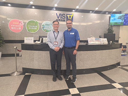
Professor Shyh-Chiang Shen, Director of GaN Programs Development (left), Maurizio Di Paolo Emilio, Marcom Director, EPC (right)
In my view, this is an important aspect of EPC's strategy. GaN performance is not determined by the transistor design alone. The ability to manufacture increasingly small and uniform devices, maintain yield, manage thermal performance and ultimately package the device effectively is becoming just as important. EPC's collaboration with Vanguard therefore goes beyond a conventional foundry relationship: it provides a manufacturing foundation for pushing its GaN technology into increasingly demanding applications.
Professor Shyh-Chiang Shen, Director of GaN Programs Development at VIS, describes the company as one of the early eight-inch GaN foundries, with in-house platforms ranging from 650 V to 1,200 V. More recently, the company has been working with EPC on low-voltage GaN technology below 100 V.
“More recently we also look at a technology by collaborating with EPC to further develop a low voltage gallium nitride technology toward less than 100 volt,” Shen said.
Moving GaN below 100 V
The lower-voltage segment presents a different manufacturing challenge from high-voltage GaN. At lower voltage ratings, designers can optimize the transistor for extremely low on-resistance and very high current, while also taking advantage of the ability of GaN to switch at high frequency.
That combination is particularly attractive in applications such as point-of-load conversion, AI processor power delivery, robotics and motor control, where the power stage must deliver large currents from a compact footprint.
The challenge is that achieving very low resistance requires increasingly small device geometries and tight control of the manufacturing process.
According to Shen, advanced photolithography is therefore a critical enabler. Moving from six-inch to eight-inch manufacturing gives the foundry access to more advanced tools and allows smaller critical dimensions.
“Vanguard as an eight-inch foundry, we are able to offer a much reduced critical dimensions for these low voltage device applications,” Shen explained.
For EPC, this capability is important because low-voltage GaN performance is strongly connected to the ability to reduce conduction losses while maintaining the high-frequency switching characteristics for which GaN is known.
A reduction in device dimensions can contribute to lower on-resistance and higher power density, but only if process uniformity and yield remain under control. The manufacturing platform therefore becomes part of the performance equation.
Eight-inch wafers: more than higher throughput
The move to eight-inch wafers is sometimes viewed primarily as a manufacturing-scale decision. However, for low-voltage GaN it also has implications for device performance and process capability.
Larger wafers provide increased throughput, but the more important advantage for advanced low-voltage devices is access to manufacturing equipment capable of controlling smaller geometries with greater precision.
Shen points to the combination of wafer size, advanced equipment and process control as a key advantage of the eight-inch platform.
For EPC, this provides a manufacturing foundation for scaling its low-voltage GaN technology without treating performance and manufacturability as separate objectives. A device designed to achieve extremely low resistance and high current capability ultimately has to deliver that performance consistently across large wafer volumes.
This becomes particularly important as GaN moves from individual high-performance applications toward broader deployment in systems such as AI servers and robotics.
Process uniformity becomes a performance parameter
At the device level, low-voltage GaN is increasingly about managing very high current in a very small area. Any variation in the process can therefore have a direct impact on electrical performance and thermal behavior.
Vanguard says it has developed processes for controlling yield and scaling devices toward higher power density.
“We also have a way to control the yield and the scaling of the device toward higher power density devices,” Shen said.
This is especially relevant to EPC because its low-voltage GaN technology is aimed at applications where every micro-ohm matters. Lower resistance reduces conduction losses, while fast switching can reduce the size of magnetic components and other elements of the power stage.
The result is a system-level advantage: higher efficiency and power density can potentially be achieved simultaneously, rather than trading one against the other.
Reliability moves from technology question to manufacturing discipline
Reliability has historically been one of the key questions surrounding the adoption of GaN. As the technology enters more demanding applications, however, the discussion is increasingly shifting toward how manufacturers can demonstrate consistent reliability at volume.
Vanguard says its experience as a long-established foundry provides an important advantage here. The company has developed monitoring systems that provide feedback to engineering teams during manufacturing.
“Vanguard is a 30-plus years, eight-inch foundry service, and we already built up a lot of monitoring systems to provide real-time feedback to the engineering team,” Shen said.
For EPC, this manufacturing discipline supports a broader strategy: GaN performance cannot be separated from repeatability and quality. As the company targets applications such as AI power and robotics, customers require not simply a high-performing transistor, but a device platform capable of consistent production.
Shen believes the industry is now reaching an important point in this process.
“Gallium nitride has reached a point that people start to recognize their long-term reliability potential,” he said, noting that the accumulation of reliability data is helping increase acceptance of the technology.
Packaging is part of the GaN architecture
The transistor is only one part of the power system. As current density increases, packaging and thermal management become increasingly important.
Even with GaN's high efficiency, power losses do not disappear. At high current, the remaining losses can still generate significant heat, and the ability to remove that heat becomes a constraint on overall power density.
“Thermal management has become a big issue not only for traditional RF GaN but also for power GaN,” Shen said.
Vanguard is therefore working with customers and packaging suppliers on different approaches, including DFN and TOLT packages as well as proprietary packaging approaches.
For EPC, packaging is already an important element of its GaN differentiation. The company's packaging has evolved specifically around the requirements of high-speed, high-current power conversion. The objective is not simply to package the transistor, but to minimize the electrical and thermal limitations between the semiconductor and the rest of the power stage.
This is particularly important for low-voltage devices. As resistance falls and current capability increases, parasitic resistance and inductance in the package and interconnects become increasingly significant relative to the semiconductor itself.
From transistor to integrated power stage
The next step could be greater integration.
Shen sees integration as one of the major directions for the GaN industry, arguing that the transistor alone cannot solve all the requirements of future power systems.
“We cannot do, like I mentioned, with GaN alone,” he said. “You have to have the packaging and all these passive components all integrated into a very compact chip or very compact circuit board.”
This direction aligns closely with EPC's strategy of moving beyond the discrete transistor toward integrated GaN power solutions.
For high-frequency applications, integration can offer several advantages. Shorter interconnections can reduce parasitic inductance, while placing the power device and associated control circuitry closer together can simplify the design of the overall switching loop.
The result can be a power stage capable of operating at higher frequency while maintaining efficiency and manageable electromagnetic behavior.
Vanguard also points to the need for collaboration with silicon-based technologies, particularly for specialized GaN gate drivers.
This highlights an important reality of next-generation power conversion: the winning architecture is unlikely to be based on the transistor alone. Semiconductor process technology, gate drive, packaging, thermal management and passive components increasingly need to be optimized as one system.
Why low-voltage GaN matters for AI and robotics
The potential applications for EPC's low-voltage GaN technology extend well beyond conventional power supplies.
Vanguard identifies AI servers and robotics as emerging areas of opportunity, alongside established applications such as lidar.
“Low voltage gallium nitride is gaining more and more acceptance in different sectors,” Shen said. “The applications can range from traditionally lidar systems, and they start to expand into the AI servers.”
Robotics may be particularly interesting because power electronics are distributed throughout the machine. Motors, actuators and local power converters all need compact, efficient and responsive power stages.
The same characteristics are increasingly important in AI infrastructure. As processor power increases, power delivery systems must handle higher currents while occupying limited board area. Reducing conversion losses and increasing switching frequency can help designers achieve greater power density.
This creates a strong fit with EPC's low-voltage GaN roadmap. Rather than positioning GaN simply as a more efficient replacement for silicon, EPC is targeting architectures where high switching speed, low resistance and compact packaging can fundamentally change the design of the power stage.
A manufacturing partnership behind the roadmap
The EPC-Vanguard relationship illustrates how the next stage of GaN development is becoming an ecosystem effort.
EPC brings device architecture, application expertise and a focus on high-performance GaN power conversion, while Vanguard contributes an eight-inch manufacturing platform, process development and high-volume foundry expertise.
Shen emphasizes that the relationship is based on long-term collaboration and openness.
“We are very happy to have EPC as our partners and to work on those advanced technology to serve the power electronics world,” he said.
That partnership becomes increasingly valuable as EPC pushes GaN into lower voltage ranges. The objective is not simply to manufacture a smaller transistor. It is to create a scalable platform capable of delivering very low resistance, high current density, high-frequency switching and reliable operation in volume.
The opportunity is significant. According to Shen, low-voltage GaN is entering applications that could become some of the defining power markets of the next decade, particularly as AI infrastructure and physical robotics expand.
“Gallium nitride will be one of the most important technologies in the next decade,” Shen said.
For EPC, the combination of its GaN device technology with an advanced eight-inch manufacturing platform provides a path to extend the benefits of GaN into a much broader range of power architectures - from AI power delivery to robotics and high-performance motor control - where efficiency, switching speed and power density are becoming increasingly difficult to achieve with conventional silicon technology.