Powering the AI Factory: How EPC GaN Solutions Supercharge the NVIDIA MGX Architecture
The digital world is entering a new AI industrial revolution, with data centers transforming into AI factories that generate intelligence at massive scale. AI is no longer just a software story; it is rapidly becoming an infrastructure story as well. Modern workloads are shifting from simple human‑to‑AI interactions toward AI‑to‑AI collaboration, where agentic models coordinate tasks, reason autonomously, and work across extremely long token sequences. This puts new pressure on infrastructure: not only do systems need more raw compute, they must also meet strict requirements around latency, thermal management, and energy efficiency. To understand how AI factories are being built in practice, NVIDIA MGX™ provides the modular foundation for scalable and flexible accelerated computing infrastructure. While MGX addresses infrastructure modularity and faster deployment, a more serious bottleneck is brewing elsewhere: power delivery. The efficiency of power conversion is critical to maintain performance and efficiency as AI systems become more complex and denser. A key enabling technology is Efficient Power Conversion’s (EPC) gallium nitride (eGaN®) solutions, which offers the efficiency, power density, and thermal performance required for next-generation AI infrastructure.
NVIDIA MGX: Modular Infrastructure for Accelerated Computing
Rather than requiring a complete hardware redesign for every new accelerator generation, NVIDIA MGX provides an open modular reference architecture spanning single-node servers, rack-scale systems, pod-level deployments, and full AI data center infrastructure.
Instead of building new platforms for each specific use case, OEMs and ODMs can leverage a standardized architectural framework that supports many different combinations of CPUs, GPUs, networking and data processing units (DPUs).
The modular approach significantly reduces non-recurring engineering (NRE) costs and accelerates time-to-market by several months. A common hardware “DNA” allows partners to reuse design elements across multiple generations of accelerated computing platforms, increasing ROI and enabling rapid system customization. MGX is optimized for x86 and Arm based server architectures and industry standards like PCIe for broad compatibility.
What makes NVIDIA MGX stand out is its flexibility. According to NVIDIA, the architecture supports more than 100 standard system configurations, allowing scalable designs that can grow from enterprise servers to large-scale AI infrastructure without a full redesign. Yet, as AI compute density continues to scale, modularity alone is no longer sufficient. The challenge increasingly shifts toward delivering power efficiently to support rapidly growing thermal and computational demands.
Third-Generation MGX Rack Architecture for Agentic AI
At the rack level, the third-generation NVIDIA MGX architecture - introduced alongside the NVIDIA Vera Rubin platform - is purpose-built to address the rapidly emerging requirements of agentic AI systems. These workloads require high throughput inference, low latency interconnects, dense CPU sandboxing, and large memory capacity for key-value cache expansion and continuous reasoning workflows.
The third-generation NVIDIA MGX rack incorporates several engineering advances in mechanical design, power distribution and thermal management. A fully modular printed circuit board (PCB)-based rack removes traditional cabling, hoses and system fans, allowing a cable-free, fanless compute environment. NVIDIA NVLink switch trays can be replaced without interrupting rack functionality providing increased resiliency and serviceability in large scale deployments.
Another key innovation is power optimizing. The dynamic power steering allows the system to intelligently distribute the available power among the CPUs, GPUs and NVLink subsystems based on workload requirements at any point in time, and the rack level capacitors help dampen sudden power spikes typical of AI inference and training workloads. The system also has 100% liquid cooling that can operate at warm-water inlet temperatures up to 45 degrees Celsius, reducing power usage effectiveness (PUE) and freeing up more energy for computation rather than cooling overhead.
The Strategic Shift to 800 VDC Power Architecture
A key element of NVIDIA’s strategy for its AI infrastructure is the use of 800 VDC power architecture. As the power density of racks increases, next generation accelerated computing requirements challenge the economic viability of traditional AC-based power delivery systems. NVIDIA’s 800 VDC approach reduces the number of power conversion stages and moves direct current distribution closer to the rack to improve efficiency and simplify data center infrastructure.
Importantly, the architecture is both forward scalable and backward compatible. New AI factories can leverage end-to-end 800 VDC distribution for maximum energy efficiency, while existing facilities can deploy hybrid architectures with MGX-compatible power racks, without sacrificing existing investments into land, power infrastructure, or building shells. The architecture also supports distributed battery backup systems which increase resiliency and enable higher density compute deployments.
As GPU power requirements scale from the 1,000 W range of the NVIDIA Blackwell architecture to the projected 6,000 W for future Feynman-class GPUs, traditional 48 VDC distribution is reaching its physical limit. Delivering 12 kW to a single NVIDIA Vera Rubin server board at 48 V would require a current of 250 A, which is impractical for standard connectors and results in massive copper losses.
To implement this high-voltage distribution, three primary architectural options have emerged, each leveraging Efficient Power Conversion (EPC) GaN technology:
- 800 VDC to 48 VDC: This approach uses a compact 800 V to 48 V converter, often located on a Power Distribution Board (PDB) or locally at the server. It allows for the continued use of traditional 48 V hardware on the server board, easing the transition to higher power levels.
- 800 VDC to 12 VDC: By converting 800 V directly to 12 V on the server board, distribution losses are reduced by four times compared to lower voltage buses. This architecture often utilizes an 8-stage ISOP configuration with 100 V or 150 V GaN devices to achieve high density within the "NVLink radius".
- 800 VDC to 6 VDC: This represents a high-efficiency path for single-stage conversion to the sub-1V levels required by the processor. While it increases distribution losses on the board, it minimizes conversion stages. This configuration benefits from EPC's latest low-voltage GaN transistors specifically designed for high-current point-of-load (POL) conversion.
800 VDC to 48 VDC
One of the most pragmatic approaches to the next generation of AI power delivery is to step down 800 VDC to 48 VDC via a compact isolated converter, which is typically located either on a Power Distribution Board (PDB) or locally inside the server rack. This architecture supports existing 48 V server ecosystems, allowing hyperscalers and OEMs to utilize mature infrastructure while scaling to substantially higher rack power densities.
From a system perspective, 48 V intermediate bus is an effective trade-off between efficiency, current handling and architectural flexibility. This allows designers to take advantage of existing server-board topologies and the familiar 48 V distribution layer with minimal disruption to the existing hardware ecosystem.
But at the semiconductor level, this stage requires devices with high switching frequencies and high power densities and without excessive thermal losses. This is where 150V GaN FETs, such as the EPC2376, can provide a benchmark solution on both primary and secondary sides of the ISOP. Compared to silicon MOSFET alternatives, these devices provide dramatically lower switching losses, negligible reverse recovery charge, and superior power density, enabling smaller magnetics, higher operating frequencies, and more compact converter implementations.
800 VDC to 12 VDC
Another more aggressive architectural approach takes 800 VDC and converts it directly to 12 VDC on the server board, dramatically reducing the number of intermediate conversion steps and improving the overall system efficiency. The most immediate benefit is in distribution: operating at higher voltage greatly reduces the current, so conduction losses are about four times less than in lower voltage bus architectures.
This topology is particularly appealing for AI accelerators where power delivery has to be performed under tight physical constraints, in particular within the so-called “NVLink radius” where proximity to GPUs is critical to minimize parasitic losses and preserve transient performance.
To achieve the required power density and thermal performance, EPC recommends an eight-stage Input-Series Output-Parallel (ISOP) architecture. This configuration alleviates the voltage stress of multiple stages, enabling the utilization of 150 V GaN devices on the primary side and 40 V devices, such as the EPC2366 on the secondary side, that inherently demonstrate improved switching characteristics and lower conduction losses than their higher-voltage counterparts. In addition to optimizing semiconductor efficiency, the ISOP approach enables easier transformer implementation, better phase interleaving, less output capacitance, and a more even distribution of thermal dissipation throughout the system - all of which are critical benefits in an AI server environment that’s increasingly power-constrained.
800 VDC to 6 VDC
At the most performance-oriented end of the spectrum, direct conversion from 800 VDC to 6 VDC represents an ultra-efficient pathway for powering modern AI processors, which ultimately require sub-1 V supply rails. By moving closer to the final operating voltage in a single isolated stage, this architecture minimizes conversion complexity and reduces the number of intermediate power stages, potentially increasing end-to-end efficiency.
The tradeoff, however, lies in on-board power distribution. Lower bus voltages increase current levels, leading to higher conduction losses across PCB traces and interconnects. Consequently, this architecture requires extremely efficient local power conversion to remain viable.
This is precisely where next-generation low-voltage GaN transistors become critical. EPC’s latest 25 V and 15 V GaN FETs,EPC2379 and EPC 2378 respectively, are optimized for high-current point-of-load (POL) conversion, provide ultra-low on-resistance, zero reverse recovery charge, and exceptional switching performance at frequencies extending into the MHz range. These characteristics enable compact, high-current POL regulators capable of efficiently delivering the ultra-low voltages demanded by GPUs and AI accelerators while maintaining high power density and fast transient response.
EPC GaN: The Technical Backbone of the ISOP Converter
The isolation stage has to be very efficient and thin to bridge the gap between 800 VDC distribution and compute level voltages. The 800 V stress is shared across several stages by stacking the inputs of multiple modular LLC resonant converters in series, allowing the system to use low-voltage GaN FETs.
Why 8-Stage ISOP with GaN is the Benchmarking Choice: The use of eight modules in an ISOP configuration provides several technical advantages over traditional single-stage designs:
- Superior Semiconductor Performance: Lower voltage GaN FETs exhibit much better Figures of Merit (FoM). For instance, the EPC2381 (Gen 7) 100 V device features an RDS(on) of only 0.8 mΩ.
- Thermal and Electrical Distribution: Spreading the conversion across eight stages allows for better thermal distribution across the PCB and a simplified transformer design.
- Reduced Ripple through Interleaving: Operating multiple modules with interleaved phases significantly lowers output-current ripple while increasing ripple frequency, which reduces the need for large, bulky output capacitors.
- Extreme Density: EPC’s surface-mount GaN devices enable converters that are incredibly thin - typically only 8 mm - making them compatible with the advanced liquid-cooled cold plates required for Rubin-class systems.
A practical implementation of this is the EPC91123, a 6 kW ISOP-based DCDC converter that converts 800 VDC to 12.5 VDC. This design achieves a peak efficiency of 98.3% and a full-load efficiency of 97%, all while occupying less than 5,000 mm2 of board space. Lab tests confirm that this architecture can handle input and output currents of up to 500 A with natural voltage balancing, eliminating the need for complex control loops (figure 1 and 2).
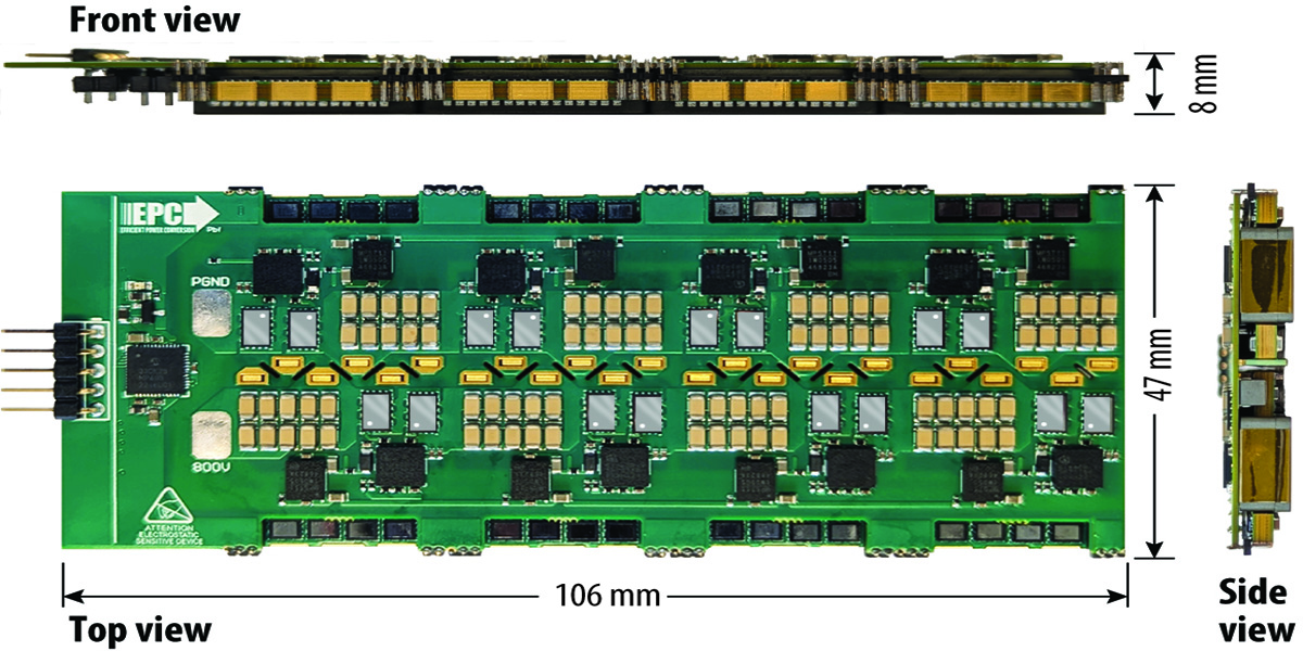
Figure 1: EPC91123 Evaluation Board
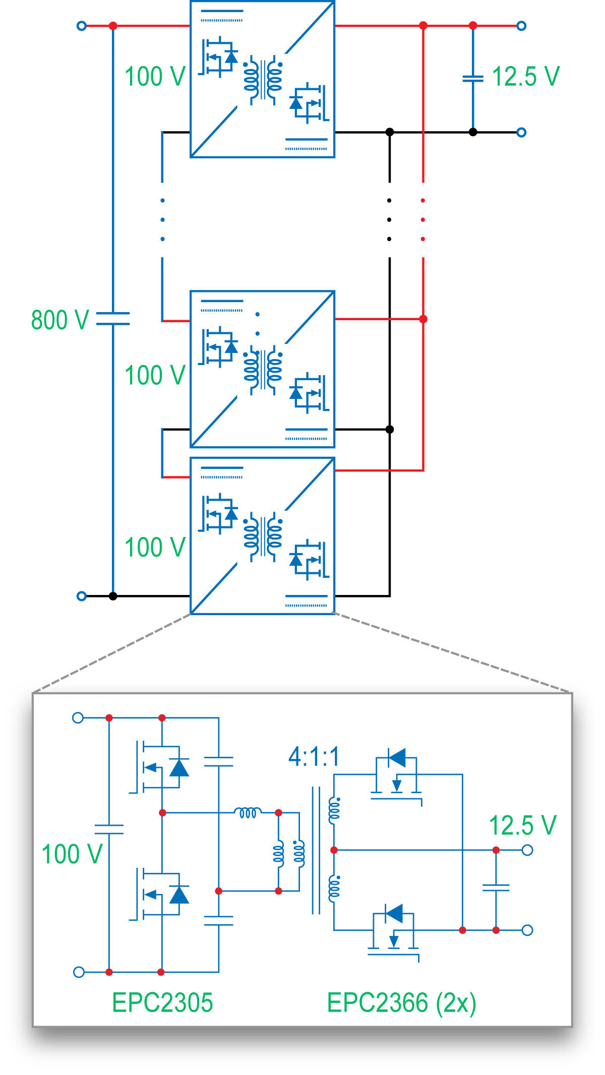
Figure 2: Block diagram of the ISOP Converter
Reimagining Intermediate Bus Conversion
EPC considers competing approaches for converters to convert 48 V rails to 12 V or 6 V outputs at the intermediate bus level, with particular focus on LLC resonant converters and hybrid switched capacitor (HSC) topologies.
EPC prefers Type I LLC architectures for the 48 V-to-12 V conversion since they have the advantage of simpler transformers and fewer winding turns compared to HSC architectures. The argument is based on the practical magnetic realization that Type I LLC topologies require fewer primary windings, fewer turns ratios and therefore less complexity while maintaining the efficiency. Such reductions are important for increasingly power-dense AI systems, where magnetic losses and transformer size are increasingly bottlenecks.
At the same time, low voltage conversion stages are also moving to 25V and 15V GaN devices for higher efficiency and density in downstream POL converters.
Point-of-Load Conversion: The Final Efficiency Battle
The final stage of power delivery - the POL regulator feeding GPUs and AI accelerators - is arguably where GaN demonstrates its greatest advantage.
EPC showcases the EPC2371, a 25 V GaN transistor optimized for high-current POL applications. The device features:
- 0.65 mΩ typical RDS(on)
- 88 A continuous current capability
- 412 A pulsed current handling
- 17 nC gate charge
- 0 nC reverse recovery charge
- Compact 2.6 mm × 3.3 mm footprint.
Efficiency tests at 700 kHz switching frequency and 0.8 V output indicate conversion efficiencies of over 90% for meaningful load ranges even without the use of heatsinks under controlled airflow conditions. These results show that GaN is capable of maintaining high efficiency even with the aggressive switching frequencies needed for modern AI loads.
For ultra-low-voltage applications, EPC’s 15 V GaN FET, EPC2370, pushes performance even further with extremely low resistance of 0.28 mΩ while still supporting high current densities. The efficiency is benchmark even up to switching frequencies above 2 MHz, which supports the notion that GaN can support higher switching frequencies and smaller passive component footprints at the same time.
This gives AI server designers the opportunity to cut PCB area dramatically, improve transient response and reduce cooling overhead.
Conclusion
As AI factories continue to scale, EPC is already looking toward the future with Gen 8 tech. Coming in late 2027, these next-generation devices will enable 3 -5 MHz high-density point-of-load (POL) solutions, further closing the gap between high-voltage distribution and the GPU. By combining the modular flexibility of NVIDIA MGX with the EPC GaN solutions, the industry can finally deliver the energy-efficient, megawatt-class racks required for the next generation of AI.
Reference
GaN Power Devices for Efficient Power Conversion, Fourth Edition - by Alex Lidow, Michael de Rooij, John Glaser, Alejandro Pozo Arribas, Shengke Zhang, Marco Palma, David Reusch, Johan Strydom.
M. Di Paolo Emilio, The Architectural Imperative of 800 VDC in Next-Generation AI Factories - Data Centre Digest
M. Di Paolo Emilio, Powering the AI Factory: The Role of 800 VDC Distribution and ISOP Converters in Next-Generation Data Centers – Data Centre Digest
Huntington, J.; Tu, M., “800 VDC Architecture for Next-Generation AI Infrastructure,”
NVIDIA White Paper, 2025.