Building the Smallest, Most Cost Effective, Highest Efficiency Non-isolated 48 V to 5 - 12 V DC to DC Converters using latest Generation 100 V eGaN FETs
GaN Talk – Rick Pierson
Apr 24, 2019
Emerging computing applications demand more power in much smaller form factors. In addition to the expanding needs of the server market, some of the most challenging applications are multi-user gaming systems, autonomous cars, and artificial intelligence. These applications are generating a demand for DC-DC converters that can squeeze onto the motherboard in close proximity to the processors.
The smallest, most cost-effective and highest efficiency non-isolated 48 V to 5 - 12 V converters, suitable for these high-performance computing and telecommunication applications, can be achieved by employing 100 V eGaN® FETs such as the EPC2045 and EPC2053.
The EPC9205 DrGaN power module, using the EPC2045 configured as a synchronous buck converter, yielded a power density of 1400 W/in3 when operating at 48 V input, 12 V output and 10 A load. It is capable of producing an output voltage ranging from 5 V to 12 V and delivering 14 A output current.
For applications requiring higher current, the EPC9093 GaN development board configured as a synchronous buck converter yields a main power stage area of only 10 mm x 9 mm − at least 2x smaller than its Si equivalent. Even at this extremely small size, it is capable of producing an output voltage ranging from 5 V to 12 V and delivering 25 A output current.
100 V EPC2045 and EPC2053 eGaN FETs
The latest generation of 100 V GaN devices increase the efficiency, shrink the size, and reduce system cost for 48 V power conversion. The EPC2045, shown in figure 1, is rated at 100 V with 7 mΩ on- resistance that can carry a continuous current of 16 A. The EPC2045 is nearly one-tenth the footprint of a comparable Si MOSFET and has lower parasitic capacitances and can switch much faster than equivalent silicon devices, yielding lower switching loss even at higher switching frequency.
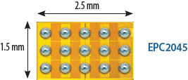
Figure 1: EPC2045 100 V eGaN FET with 7 mΩ on-resistance
The EPC2053, shown in figure 2, is rated at 100 V with 4 mΩ on-resistance that can carry a continuous current of 32 A. The EPC2053 has lower parasitic capacitances and on-resistance than its silicon counterparts, yielding faster switching speed and lower power losses even at higher switching frequencies. These characteristics enable increasing the output power while shrinking the volume of the converter.
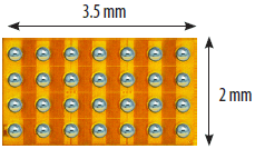
Figure 2: EPC2053 100 V eGaN FET with 4 mΩ on-resistance
EPC9205 power module showcasing the EPC2045
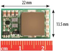
Figure 3: EPC9205 development board
The EPC9205 power module, shown in figure 3, is configured as a synchronous buck that is fitted with two EPC2045 eGaN FETs. The EPC9205 features the uP1966A half-bridge gate driver IC from uPI Semiconductor Corp., input and output filters, as well as current and temperature sensing. The high-frequency capability of eGaN FETs greatly reduces the filtering requirements, allowing for an optimized output filter inductor with much smaller size and lower loss.
When stepping down 48 V to 12 V at 700 kHz, the EPC9205 achieves a peak efficiency of 96% at 10 A load, with a maximum FET temperature of 100ºC under 400 LFM airflow. Figure 4 shows the power efficiency curve for 12 V load up to 15 A output current. The same EPC9205 is also capable of producing output voltages as low as 5 V. Figure 5 shows the efficiency as a function of load current at 5 - 12 V output when operating at 500 kHz.
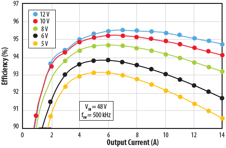 Figure 4: EPC9205 efficiency vs output current for 48 VIN to 12 VOUT when operating at 500 kHz
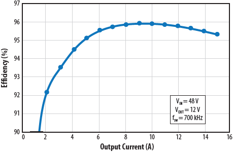 Figure 5: EPC9205 efficiency vs output current for 48 VIN to 12 VOUT when operating at 700 kHz
EPC9093 GaN development board showcasing the EPC2053
The EPC9093 development board, with the block diagram schematic shown in figure 6, is configured as a synchronous buck converter that is fitted with two EPC2053 eGaN FETs. The EPC9093, with the main power stage shown in Figure 8, also features the uP1966A half-bridge gate driver IC from uPI Semiconductor Corp. The main power stage occupies only 10 mm x 9 mm and is at least 2x smaller than an equivalent Si MOSFET power stage. The high-frequency capability of eGaN FETs significantly reduces the filtering requirements, allowing for a significant size and loss reduction in the output filter inductor as well.
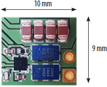
Figure 6: The EPC9093 development board fitted with the EPC2053
When stepping down 48 V to 12 V at 700 kHz switching frequency, the EPC9093 achieves a peak efficiency of 97% at 15 A load and maintains an efficiency above 96.5% at 25 A load. Figure 7 shows the power efficiency up to 25 A output current for 5 V, 9 V, and 12 V output at 700 kHz operating frequency. Figure 8 shows the efficiency as a function of the load current for 5 V, 9 V, and 12 V output at 1 MHz operating frequency. The peak efficiency is still above 96% when the operating frequency is increased to 1 MHz.
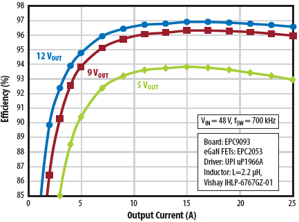 Figure 7: EPC9093 efficiency vs output current for 48 VIN to 12 VOUT operating at 700 kHz
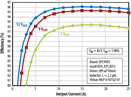 Figure 8: EPC9093 efficiency vs output current for 48 VIN to 12 VOUT operating at 1 MHz
Conclusions
Migrating an intermediate 48 V to 5 - 12 V bus converter design from silicon MOSFETs to eGaN FETs offers a reduction in both size and cost while maintaining or exceeding efficiency targets. Table 1 shows the bill of materials of an eGaN FET-based 48 V to 12 V, 25 A buck converter that yields a cost per watt of less than $0.03. This same bill of materials can be used for output voltages as low as 5 V
The eGaN FET-based 48 V to 5 - 12 V, 25 A load converter was demonstrated to yield 5 V, 9 V and 12 V output with a peak efficiency of 97%, a main power stage at least 2x smaller than Si equivalents, and a cost that can go below $0.03 per watt when operated with a 12 V output.
The latest 100 V GaN devices increase the efficiency, shrink the size, and reduce system cost in 48 V conversion, thus meeting the challenging demands of high-density computing.
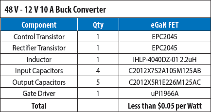 Table 1: Bill of Materials for an eGaN FET based 48 V to 12 V, 25 A converter based on 500 k unit pricing