From 800 V to Core: Where Is the Next Breakthrough in AI Server Power Delivery?
GaN Talk – Maurizio Di Paolo Emilio
Oct 02, 2026
Qian Luo, Author, WBG TechnoBite
At PCIM Asia 2026, EPC presented its Gen 8 monolithic GaN power stage for AI processor power delivery.
Developed by EPC for high-frequency multiphase POL / IVR applications on next-generation AI processors, Gen 8 integrates half-bridge power switches, high-speed gate drivers, bootstrap circuitry, level shifting, and logic on the same GaN die. With lower charge, faster switching, and stronger overvoltage capability, it targets operation from a 6 V input at frequencies approaching the 10 MHz class. The system-level significance is not simply a lower component count: integration reduces drive-loop parasitics and noise sensitivity, while allowing the control side to use high-speed processes better suited to extensive digital functionality, enabling more phases and denser processor-side placement.
Seen only as a new device generation, however, the broader context is missed. EPC's Gen 7, Gen 8, and reference designs now span a continuous power-delivery path from the 800 V rack bus through intermediate rails to the final processor-side conversion stage.
800 VDC first addresses rack-level distribution. As the voltage is stepped down to 50 V, 12 V, and approximately 6 V, the problem shifts toward board-level conversion, the PDN, packaging, and cooling. At a 0.5-0.6 V processor core, current demand is moving from several kiloamperes toward 10,000 A. At that point, system performance depends not only on the efficiency of any one conversion stage, but on where very high current first appears, how far it must travel, and whether the final stage can be placed close to the GPU.
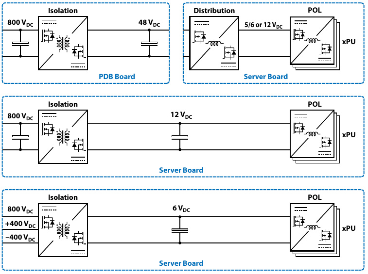
Figure 1. Three power-delivery paths from 800 VDC to 48 V, 12 V, and 6 V. Source: EPC WP020.
Why Is the Final Stage Becoming the New System Constraint?
800 V can sharply reduce rack-bus current. At the same 200 kW, current on an 800 V bus is roughly 1/16 of that on a 48 V bus. But the current does not disappear. It returns - in much more concentrated form - as the voltage approaches the processor core.
WBG TechnoBite: What has changed in AI power delivery - and why is the final stage now the bottleneck? At PCIM Asia, EPC's presentation moves from 800 V conversion through Gen 7 devices to a 10 MHz Gen 8 POL stage close to the GPU. From EPC's perspective, what has changed in AI-accelerator power demand that makes the final voltage-regulation stage a new system bottleneck? Which constraints are now driving the architecture most strongly - current density, transient response, PDN loss, space/cooling, or another factor?
EPC:
Power is the driving force behind these changes. As rack power rises, a 50 V bus bar is no longer adequate, which is why the 800 V architecture is being introduced. Moving from SPS-based lateral power delivery to VPD removes most of the massive PDN loss associated with roughly 100 µΩ. At 2,000 A, the remaining 10 µΩ of PDN resistance is manageable, corresponding to about 40 W of loss. At 10,000 A, the same 10 µΩ creates 1,000 W of loss inside the motherboard. Moving power delivery to the other side of the PCB removes this 10 µΩ PDN path. As discussed in the Google paper, conduction loss scales with the square of current.
These numbers explain why the final stage is becoming a structural problem rather than only a device problem. A 10 µΩ PDN is still manageable at 2,000 A; at 10,000 A, however, it leaves 1 kW of heat inside the motherboard. Chips and regulators can be given dedicated cooling interfaces, while distributed conduction loss inside the PCB is much harder to remove.
In conventional lateral power delivery (LPD), multiphase VRs are arranged around the ASIC and current travels across the plane of the motherboard into the package. Vertical power delivery (VPD) moves the power module to the back side of the processor so current enters the package along the Z-axis. The change is not simply component placement: it shrinks centimeter-scale lateral paths into millimeter-scale vertical paths while releasing the chip perimeter for high-speed I/O and other components.
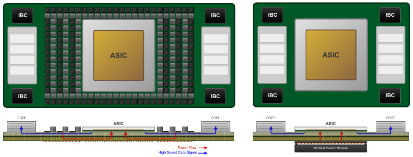
Figure 2. Board-level comparison of lateral and vertical power delivery. Source: Zichao Ye et al., IEEE TCPMT, 2026 (CC BY 4.0).
50 V, 12 V, or Approximately 6 V?
Once 800 V enters the rack, there is no single mandatory next voltage. Converting to 50 V preserves the existing bus-bar and server power chain; stepping directly to 12 V or approximately 6 V moves the point at which low-voltage, high-current distribution begins closer to the server board and the processor.
WBG TechnoBite: How should the intermediate rail be chosen when the whole 800 V-to-GPU chain is optimized? EPC has demonstrated 800 V-to-50 V, 12.5 V and 6.25 V paths. If a server designer optimizes the complete path from 800 V to the GPU rather than the efficiency of one converter, how should the intermediate voltage be chosen? Under what conditions is 48/50 V, 12 V or approximately 6 V the better architecture, and does Gen 8 materially shift that balance toward a lower rail?
EPC:
It is about the power. At today's power levels, the system is still manageable, and using the existing rack system is easier for the supply chain. An 800 V-to-50 V architecture continues to use the traditional bus bar. If power is not too high, the system can afford the bus bar plus a second conversion stage to 12 V or 6 V. For next-generation, higher-power GPUs, 800 V-to-12 V or 800 V-to-6 V is more efficient.
12 V is more traditional. A 6 V rail enables more efficient and higher-density POL conversion. As power continues to rise, 6 V will dominate in order to improve POL current density. For now, 12 V and 6 V will coexist, and different customers have different preferences.
EPC's answer brings the choice back to total system power and supply-chain constraints rather than imposing a fixed ranking among the three voltages. Fifty volts extends the existing system; 12 V preserves a mature board-level ecosystem; approximately 6 V improves the conversion ratio of the final POL stage and may eliminate the 12 V-to-6 V stage, but it requires conversion to be physically close to the load.
Gen 7 GaN and ISOP LLC reference designs make these paths practical. EPC91123, for example, uses eight modules in input-series/output-parallel configuration, effectively dividing 800 V-to-12.5 V into eight 100 V-to-12.5 V conversion cells. The 6 kW reference design reaches 98.2% peak efficiency at an overall height of about 8 mm. EPC's 800 V-to-6 V design reaches roughly 98% peak efficiency and 97% full-load efficiency at 6 kW.
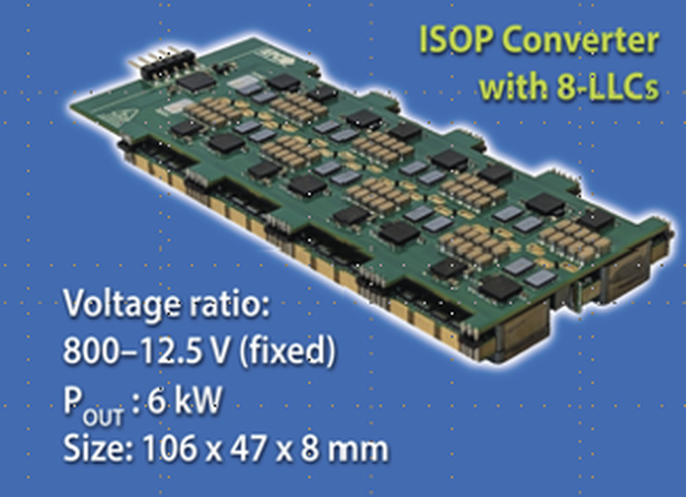
Figure 3. EPC91123 800 V-to-12.5 V / 6 kW ISOP LLC reference design. Source: EPC.
The benefits of approximately 6 V also come with a clear boundary condition. Six kilowatts at 6 V corresponds to roughly 1,000 A. Google's VPD study notes that PCB losses rise rapidly as the 6 V-bus current approaches 1,000 A, making IBC placement critical; the IBCs must sit close to the VPM. In other words, approximately 6 V behaves more like a near-load voltage node than a general-purpose rail that can be distributed over long distances across the server board. For the 12 V versus 6 V architecture comparison, see Figure 1.
What Does Gen 8 Integration Change?
As the final stage enters the multi-kiloampere range, phase count continues to rise. At that point, device performance is only the foundation; drive, control, noise, phase density, and local interconnect increasingly determine what can actually be implemented.
WBG TechnoBite: What does Gen 8 integration change at the system level? Gen 8 integrates the GaN power devices with gate drive, bootstrap, level shifting and logic. In practical design terms, what limitation does this integration remove compared with a discrete Gen 7 implementation? What new design freedom does it create for switching frequency, phase density, layout and placement near the GPU?
EPC:
High-current-density IVRs require many phases. A discrete implementation using Gen 7 is not practical and is sensitive to noise. Full integration allows the controller to use a high-speed digital process, which is important because the controller requires a large amount of digital functionality. A discrete Gen 7 implementation would force the use of high-voltage BCD, which is much slower. In addition to integration, Gen 8 has a much better FOM, which is critical at 10 MHz.
The system value is therefore not simply a lower component count. A multiphase IVR must compress the power stage, drive, and control functions close to the processor. As phase count rises, drive-loop parasitics, timing consistency, and noise coupling become progressively harder to manage. EPC frames Gen 8's role in two parts: first, pull the power and drive functions into a denser integrated unit; second, allow the control side to move to a high-speed process better suited to extensive digital functionality.
Why Target 10 MHz?
Higher frequency allows smaller magnetics and faster transient response, but it also raises switching loss and thermal density. The real question is not simply whether 10 MHz can be reached, but whether the space and thermal conditions around the processor have already pushed the design into that frequency range.
WBG TechnoBite: What is the real engineering trade-off behind 10 MHz-class regulation? EPC highlights 10 MHz-class regulation as a route to higher current density and closer POL placement. What is the engineering trade-off behind moving from today's few-megahertz operation toward 10 MHz? At what point do smaller magnetics, faster transient response and shorter PDN paths outweigh the added switching and thermal losses, and what operating range does EPC currently regard as practical?
EPC:
Moving closer to the GPU means extremely tight space, very little capacitance, and a difficult thermal environment. 10 MHz is the minimum frequency needed to make the inductor small enough to fit under the GPU. It also enables fast transient response with reasonable efficiency. The hard part is switching at 10 MHz from a 6 V input. Silicon FinFETs operate at 1.8 V and 3.3 V, which creates very large input currents, and there is no single-stage 800 V-to-3.3 V solution today. A 6 V BCD process is not very efficient. GaN can easily handle a 6 V input and tolerate 30 V voltage spikes, whereas BCD has much less voltage margin. Six volts is an ideal voltage node for GaN, and GaN's FOM enables efficient switching at 6 V and 10 MHz.
This answer ties 10 MHz and 6 V to the same physical constraint. Frequency must be high enough to make the inductor fit within the limited height behind the GPU, while the input voltage cannot be so low that upstream current becomes even larger. In WP020, EPC's current result is a 6 V-to-0.9 V GaN POL operating at up to 3 MHz with efficiency of roughly 89%; 10 MHz is identified as the next development milestone. Gen 8 is intended to put the FOM, integration, and control capability required for that frequency range into the same power stage.
What Still Has to Change Before Reference Designs Become Real Servers?
800 V, approximately 6 V, VPD, and Gen 8 will not all arrive in one step. IBCs can be introduced first as modules on the server board; IVR, because it moves power conversion much closer to the package, requires the chip, package, motherboard, control, and cooling system to evolve together.
WBG TechnoBite: What must change in a real server before this architecture can scale? As GPU current moves into the multi-kiloampere range, what becomes the dominant obstacle to scaling this architecture in a real server: the regulator itself, board/package PDN, current extraction, cooling, control or reliability? What changes will customers need to make in server-board or package-level power delivery to realize the benefit of Gen 8, and what technical validation still needs to be completed before this approach can be broadly deployed?
EPC:
Everything has to evolve over time. 800 V buys a lot of time. The path from 800 V to 6 V can gradually move from two stages to a single stage. At the POL, power delivery transitions from lateral to VPD to VPM (see the Google paper), and then to IVR. Once the technical issues are resolved and performance is proven, IBC modules can be accepted relatively quickly through ODMs. IVR requires deeper system-level involvement. Everything around the GPU has to change, and system risk must be managed. We expect the bottleneck to emerge in 2028-2029, so proof-of-concept work and IVR development should already be well under way now.
This is not a roadmap that can be advanced by power devices alone. IBCs can still follow a modular adoption path. VPM and IVR, by contrast, change component placement on both sides of the motherboard, cold-plate structure, TIM design, board warpage, solder-joint reliability, and package-level power delivery. Google's VPM prototypes also show that the production boundary for high-phase-count vertical power delivery now extends into mechanical and manufacturing considerations.
EPC's timing is equally important: 800 V first creates headroom in rack-level distribution; in EPC's view, the processor-side bottleneck becomes more visible in 2028-2029. The task today is therefore not to assume that every architecture changes immediately, but to begin proof-of-concept work and cross-layer coordination for 800 V-to-6 V, VPD/VPM, and IVR early enough.
Closing Note
From 800 V to the core, the system is not a chain of independent converters. The 800 V architecture determines how power is distributed within the rack. The choice among 50 V, 12 V, and approximately 6 V determines where low-voltage, high-current delivery begins. VPD and VPM determine how current passes through the motherboard and package. Gen 8 and 10 MHz-class operation address the final stage closest to the processor.
AI server power delivery is moving away from "choosing a device or topology" toward coordinating voltage hierarchy, physical placement, PDN design, cooling, control, and manufacturing. The value of GaN in that transition is its ability to move conversion closer to the load at higher frequency and higher density. Whether the architecture ultimately works, however, depends on the entire power-delivery chain evolving together.
Sources
- Efficient Power Conversion (EPC), "WP020: GaN-Based Power Delivery in AI Data Centers," August 2026.
- EPC Technical Team, written technical Q&A for "From 800 V to Core," September 2026.
- Jason Zhang, EPC, "EPC New Products and High-Density DC-DC Converters," PCIM Asia 2026, August 27, 2026.
- Zichao Ye et al., "Towards 10kAmp AI Chip: A System Perspective from Lateral to Vertical Power Delivery," IEEE Transactions on Components, Packaging and Manufacturing Technology, DOI: 10.1109/TCPMT.2026.3716571 (CC BY 4.0).
- Maurizio Di Paolo Emilio, "EPC’s GaN Roadmap Comes Into Focus Ahead of PCIM Asia," August 2026.
- EPC91123 product page and evaluation-board materials, Efficient Power Conversion (EPC).