Forget Everything You Thought You Knew About Semiconductors
GaN Talk – Alex Lidow, Ph.D.
Oct 13, 2016

In past postings, we looked at the applications that have emerged because of new capabilities available with GaN technology. We also discussed the transformational nature of some of these applications in areas like medicine, telecommunications, human-machine interfaces, and the delivery of electrical power itself (wireless power transfer). GaN technology is entering an era similar to the 80’s and 90’s when the utility of technological improvement was apparent across broad commercial markets. Consequentially, consumers will be willing to pay a premium for the life-style enhancements enabled by these improvements thereby accelerating growth of GaN applications for the foreseeable future.
But, to fully understand how gallium nitride-based technologies really shake the foundations of our silicon-based world, we need to analyze the cost of the GaN supply chain in conjunction with its accelerated growth rate and to examine how the financial metrics are being reset.
Capital
Today, semiconductor-based companies require large amounts of capital to expand or even maintain their revenue base. New wafer fabrication facilities cost multiple billions of dollars to build and equip. Additionally, design software and test hardware have become significant in the capital budget. Each new generation of technology requires a new suite of tools that can cost billions of dollars before the first test chip even rolls off the production line.
In 2013 the industry as a whole realized just $0.24 of incremental revenue for every dollar spent on capital equipment. It’s hard to make an adequate return on investment with this magnitude of capital intensity.
New Product Development
Whether a company has its own wafer fab, or is fabless, new products require a sizable new research and development investment. One of the largest investments required for new product development is the set of photolithographic (or photo) masks that are used to imprint the circuit images of the device onto the silicon wafer. Advanced discrete transistors (such as eGaN® FETs) may require as few as 10 photomasks, with advanced integrated circuits needing 35 or more.
Moore’s Law (the doubling of the number of transistors on a single chip every two years) depends upon the continuous reduction in a device’s feature sizes to maintain positive momentum in both cost and performance. However, as feature sizes shrank from 0.5 microns (500 nm) to 0.045 microns (45 nm) over the past 20 years, the cost to produce these photomasks super-scaled . Other development costs have also escalated, and the overall bill for an advanced silicon-based device, now in the 10’s to 100’s of millions of dollars, has become unaffordable to all but the well-funded, established companies. Similar to investment in new plant and equipment, new products are the fuel for the semiconductor industry’s growth, and, as the costs escalate, the number of new products (and their innovative contribution) decreases.
Industry Growth
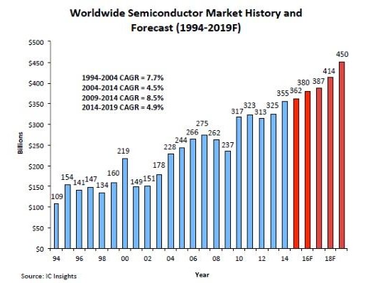
Since the year 2000, the industry as a whole has grown at only a 5% annual rate as compared to 22% in the 1980’s. The semiconductor “go-go years” of the 80’s have been replaced by the more sedate, incremental growth rate of a mature industry – with fewer and fewer bright lights from product innovation.
Low Investment Returns
As a result of the increased capital intensity, skyrocketing cost of product development, reduced product innovation, and slower revenue growth, it should be expected that the investment returns would also be reduced. That, in fact, is true. Using the Philadelphia Semiconductor Index (SOX) as the proxy for return on investment in the industry, returns can be compared against the broader Standard and Poor’s 500 index.
From 1995 to 2000, the SOX index grew 513% from 127 to 778, compared with the S&P500, which grew 156% from 544 to 1394. Once the bubble burst in 2000, however, the returns were drastically reduced and never again beat the S&P500. In fact, from January 2000 to August 2015 the SOX under performed the S&P500 by 86 percentage points!
Enter Gallium Nitride

GaN technology is remarkable in that this new semiconductor material changes the game on so many fronts. GaN has superior crystal properties that enable a performance advantage over silicon of as much as 6000:1 (GaN devices on the market today already show a 10:1 advantage and are rapidly improving).
This significant performance advantage of GaN can be realized using the existing trailing-edge silicon infrastructure. Capital spending needed for growth is vastly reduced as a result. New capital requirements are less than $1 for every $10 of new revenue. This is 40 times better than the industry average. New product developments, by virtue of the fact that gallium nitride’s superior crystal properties rely less on super-tiny feature sizes, cost less than $20k to get to first samples. This cost reduction creates an environment where numerous new products can be proliferated with very little investment risk.
Finally, and perhaps most importantly, GaN is facing a period of very rapid growth. This growth is coming from both the replacement of lower performing and higher cost silicon devices and from emerging applications that are enabled by GaN’s superior performance. Efficient Power Conversion forecasts that by 2018 half of our projected revenues will come from emerging applications such as LiDAR, Envelope Tracking, various medical applications, and Wireless Power – applications that are in their infancy today, but are exploding on the market.
Forget What You Thought You Knew
Capital intensity, high product development costs, and slowing end-markets are markers of a mature industry with sedate investment returns. This is the case for the venerable silicon-based semiconductor market today.
GaN technology provides the opportunity to recapture the early days of silicon where new markets were discovered almost every day and the cost to develop a superior product is small compared to the benefits realized by that product. No doubt there will be many players on the GaN playing field, but the big winners will be the early GaN-focused entrants that are agile, innovative, and willing to take some risk.